Semiconductor device having copper lines with reduced electromigration using an electroplated interim copper-zinc alloy film on a copper surface
a technology of copper-zinc alloy film and semiconductor device, which is applied in the direction of semiconductor/solid-state device details, electrolysis components, electrolysis processes, etc., can solve the problems of less desirable as a candidate for these higher-density devices, corrosion, diffusion into silicon, etc., to improve the reliability of cu interconnection, enhance the effect of electromigration resistance and improve corrosion resistan
- Summary
- Abstract
- Description
- Claims
- Application Information
AI Technical Summary
Benefits of technology
Problems solved by technology
Method used
Image
Examples
first embodiment
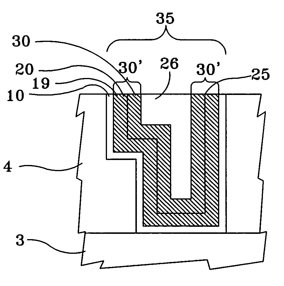
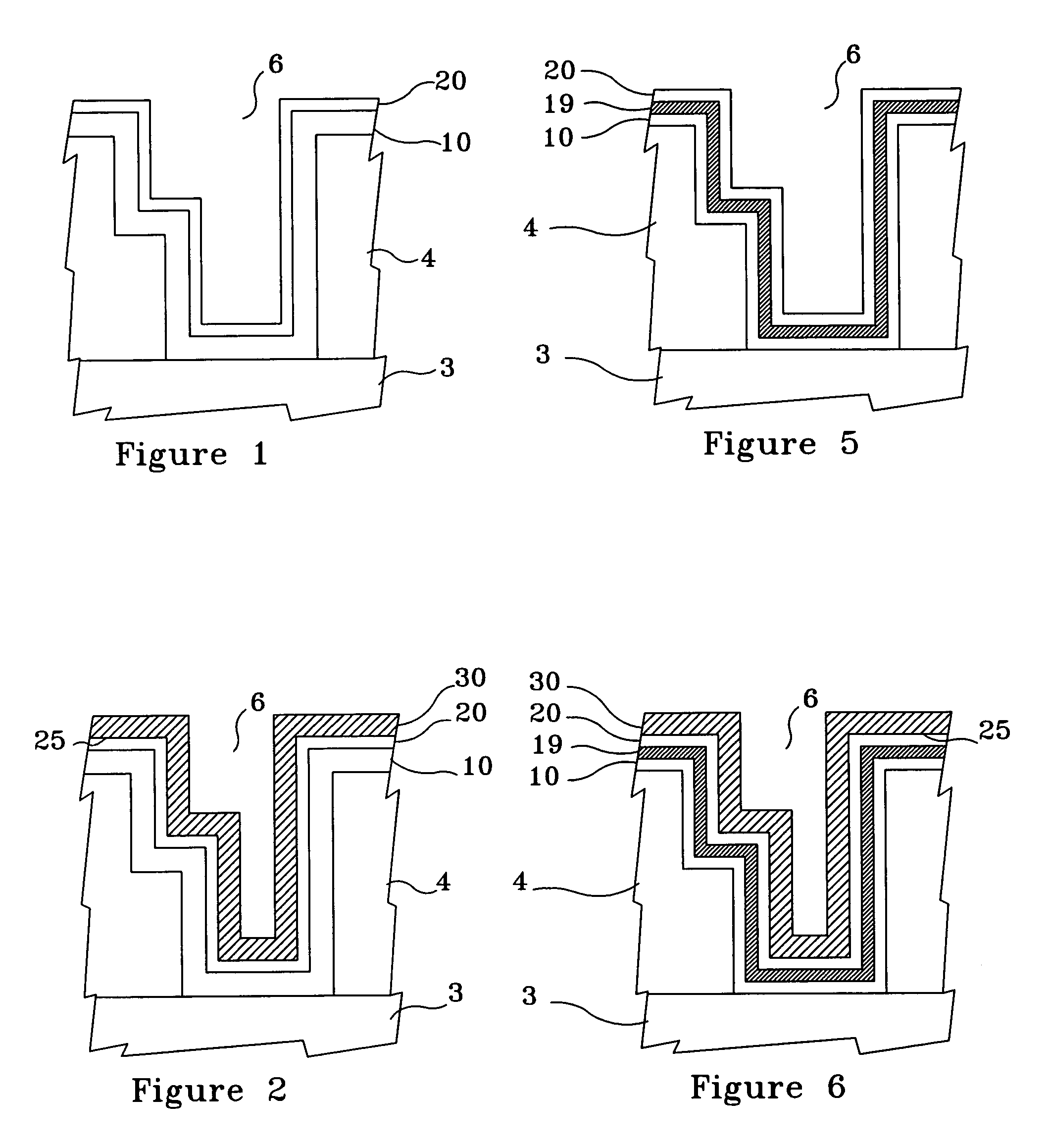
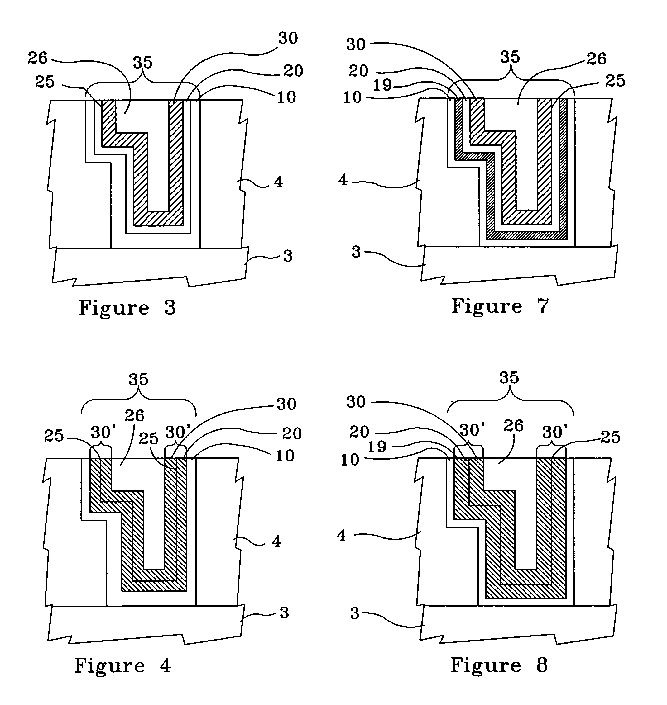
[0028]FIG. 1 illustrates, by example only, a cross-section of a Cu interconnect line 3, comprising Cu, formed on a semiconductor substrate 4 and acting as the bottom portion of a via 6, the via 6 having a optional barrier layer 10, comprising at least one material selected from a group consisting essentially of titanium silicon nitride (TixSiyNz), tantalum nitride (TaN), and tungsten nitride (WxNy), formed therein and a Cu surface 20, such as a blanket Cu seed layer and a partial thickness plated Cu layer, formed on the optional barrier layer 10, in accordance with the present invention.
[0029]FIG. 2 illustrates a cross-section of the Cu interconnect line 3 formed on a semiconductor substrate 4 and acting as the bottom portion of a via 6, the via 6 having the optional barrier layer 10 formed therein and the Cu surface 20 formed on the optional barrier layer 10, as shown in FIG. 1, having an interim conformal Cu—Zn alloy thin film 30 formed and annealed on the Cu surface 20, in accord...
second embodiment
[0032]FIG. 5 illustrates, by example only, a cross-section of a Cu interconnect line 3 formed on a semiconductor substrate 4 and acting as the bottom portion of a via 6, the via 6 having an optional barrier layer 10, comprising at least one material selected from a group consisting essentially of titanium silicon nitride (TxSyNz), tantalum nitride (TaN), and tungsten nitride (WxNy) in a thickness range of approximately 10 Å to approximately 30 Å, formed by a technique such as atomic layer deposition (ALD), atomic layer chemical vapor deposition (ALCVD), or chemical vapor deposition (CVD), an optional underlayer 19, comprising at least one material selected from a group consisting essentially of tin (Sn) and palladium (Pd) in a thickness range of approximately 15 Å to approximately 50 Å, formed on the optional barrier layer 10, and a Cu surface 20, comprising electroless Cu in a thickness range of approximately 30 Å to approximately 100 Å, formed on the optional underlayer 19, in acc...
PUM
| Property | Measurement | Unit |
|---|---|---|
| volume | aaaaa | aaaaa |
| volume | aaaaa | aaaaa |
| concentration | aaaaa | aaaaa |
Abstract
Description
Claims
Application Information


