Photomask for eliminating antenna effects in an integrated circuit and integrated circuit manufacture with same

a technology of integrated circuits and antenna effects, applied in the field of photolithography, can solve the problems of time-consuming editing of layout databases, excessive charge build-up in polysilicon gates, and the inability to eliminate so as to increase the antenna ratio, reduce the disadvantages and problems of eliminating antenna effects in integrated circuits, and eliminate the effect of the effect of the effect of the antenna

Inactive Publication Date: 2005-12-20
CELERICS TECH
View PDF43 Cites 278 Cited by
  • Summary
  • Abstract
  • Description
  • Claims
  • Application Information

AI Technical Summary

Benefits of technology

[0006]In accordance with the present invention, the disadvantages and problems associated eliminating antenna effects in an integrated circuit have been substantially reduced or eliminated. In a particular embodiment, a photomask is formed by using a mask pattern

Problems solved by technology

During a fabrication process for an integrated circuit, various plasma etching and ion implantation techniques may be used, which may cause a charge to build up in a polysilicon gate.
However, if the metal area is large compared to the polysilicon to which it is connected, there may be sufficient charge build up to degrade and even damage the polysilicon gate.
The process of editing the layout database may be time consuming since the designer must create space for additional polygons, place the polygons in t

Method used


Image

  • Photomask for eliminating antenna effects in an integrated circuit and integrated circuit manufacture with same
  • Photomask for eliminating antenna effects in an integrated circuit and integrated circuit manufacture with same
  • Photomask for eliminating antenna effects in an integrated circuit and integrated circuit manufacture with same

Examples


Embodiment Construction

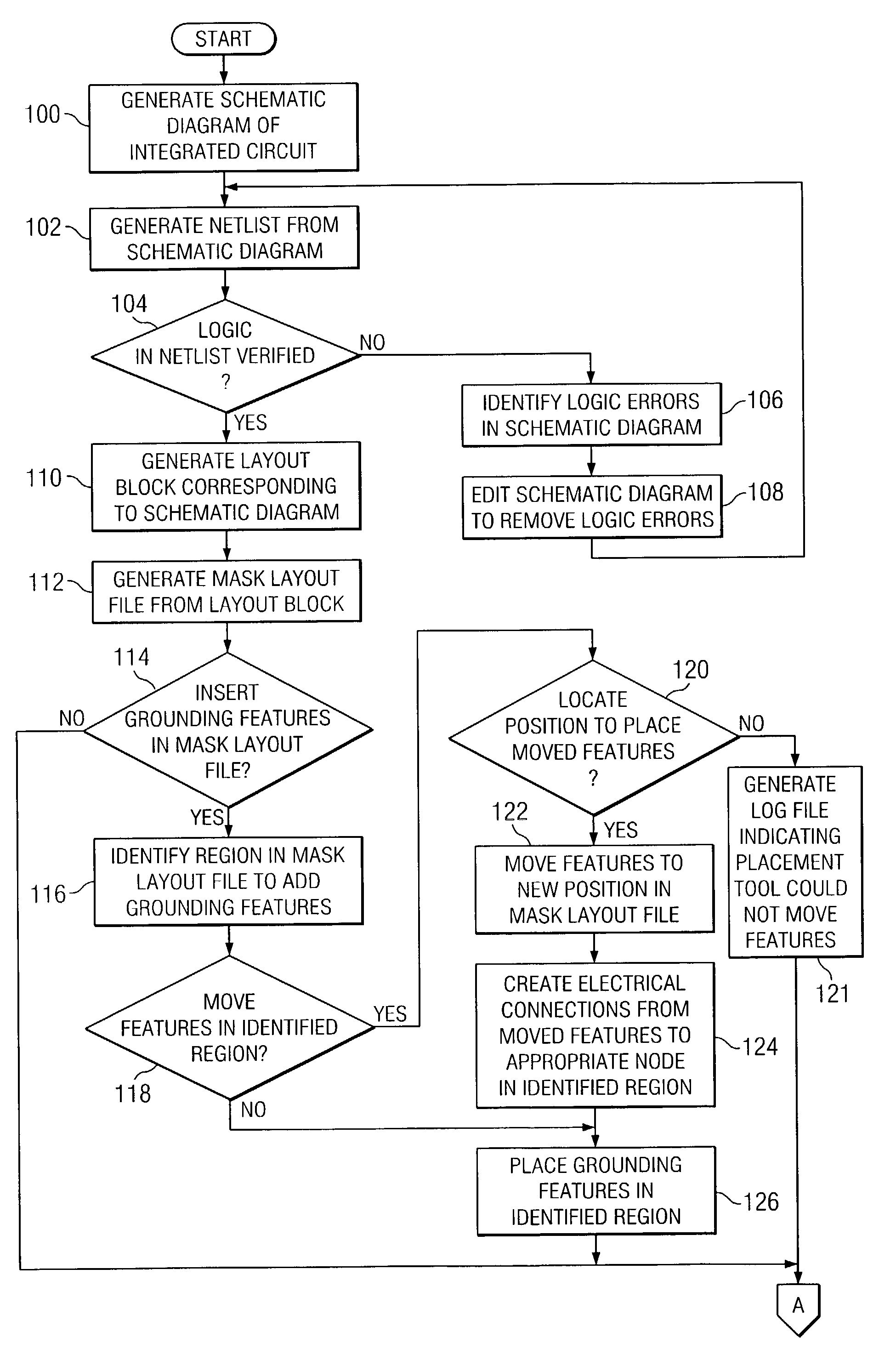
[0020]Preferred embodiments of the present invention and their advantages are best understood by reference to FIGS. 1 through 7, where like numbers are used to indicate like and corresponding parts.

[0021]As the number of transistors on an integrated circuit continues to increase, the design process for the integrated circuit becomes more complex. For example, an increasing number of transistors may require additional layers to form the integrated circuit on a semiconductor wafer. Each layer associated with the integrated circuit may include one or more design rules for the individual layer in a desired manufacturing process. The number of design rules for the desired manufacturing process, therefore, increases with the number of layers formed on the semiconductor wafer.

[0022]A design rule typically defines the minimum or maximum allowable dimension for a feature fabricated on a specific layer. For example, an integrated circuit may include, among other layers, a diffusion layer that...


PUM


Abstract

A photomask for eliminating antenna effects in an integrated circuit and integrated circuit manufactured with the photomask are disclosed. The photomask includes a substrate and a patterned layer formed on at least a portion of the substrate. The patterned layer may be formed using a mask pattern file created by analyzing a pattern in a mask layout file to identify a region including an antenna ratio less than a first design rule. A feature located in the identified region is moved based on a second design rule from a first position to a second position in the mask layout file to create a space in the identified region. A grounding feature is placed in the space and automatically connected to a gate feature in the mask layout file such that the antenna ratio is increased to greater than or approximately equal to the first design rule.

Description

RELATED APPLICATIONS[0001]This application is a continuation-in-part of U.S. patent application Ser. No. 09 / 684,793, filed Oct. 10, 2000 and entitled “AUTOMATIC DIFFUSION DIODE (‘ANTENNA’) CONSTRUCTION, PLACEMENT AND CONNECTION IN IC MASK LAYOUT DATABASE METHOD AND COMPUTER SOFTWARE”, now abandoned.TECHNICAL FIELD OF THE INVENTION[0002]This invention relates in general to the field of photolithography, and more particularly to a photomask for eliminating antenna effects in an integrated circuit and integrated circuit manufactured with the photomask.BACKGROUND OF THE INVENTION[0003]A typical semiconductor design process includes numerous steps. Initially, a circuit designer prepares a schematic diagram that includes logical connections between logic elements that form an integrated circuit. The schematic diagram is then tested to verify that the logic elements and associated logical connections perform a desired function. Once the circuit is verified, the schematic diagram is convert...

Claims


Application Information

Patent Timeline
IPC IPC(8): G03F1/14G06F17/50G06F19/00G21K5/00
CPCG03F1/144G03F1/36G06F17/5081G06F30/398
Inventor RITTMAN, DANNYOREN, MICHA
Owner CELERICS TECH
Why Eureka
Try Eureka