Semicondutor device having ferroelectric capacitor and hydrogen barrier film and manufacturing method thereof

a technology of ferroelectric capacitor and semiconductor device, which is applied in the direction of transistors, instruments, picture interpretation, etc., can solve the problems of undesirable problems, deterioration of properties, and inability to use simple and reliable techniques, and achieve excellent ferroelectric capacitor, effective recovery of ferroelectric properties, and better stopping function

Inactive Publication Date: 2006-01-03
KK TOSHIBA
View PDF14 Cites 51 Cited by
  • Summary
  • Abstract
  • Description
  • Claims
  • Application Information

AI Technical Summary

Benefits of technology

[0029]By thus increasing the contact area with the upper electrode, the ferroelectric property is effectively recovered by recovery annealing in the process of making the contact hole, and an excellent ferroelectric capacitor can be obtained.
[0030]In the present invention, the hydrogen barrier film formed on the capacitor can be used also as a stopper in the process for leveling the inter-layer insulating film on the hydrogen barrier film. Additionall

Problems solved by technology

Heretofore, however, there have been no simple and reliable techniques.
Ferroelectric capacitors involve various problems, such as deterioration of the property caused by process damage, which must be removed, in addition to characteristic deterioration due to reduction by hydrogen.
On the other hand, th

Method used


Image

  • Semicondutor device having ferroelectric capacitor and hydrogen barrier film and manufacturing method thereof
  • Semicondutor device having ferroelectric capacitor and hydrogen barrier film and manufacturing method thereof
  • Semicondutor device having ferroelectric capacitor and hydrogen barrier film and manufacturing method thereof

Examples


first embodiment

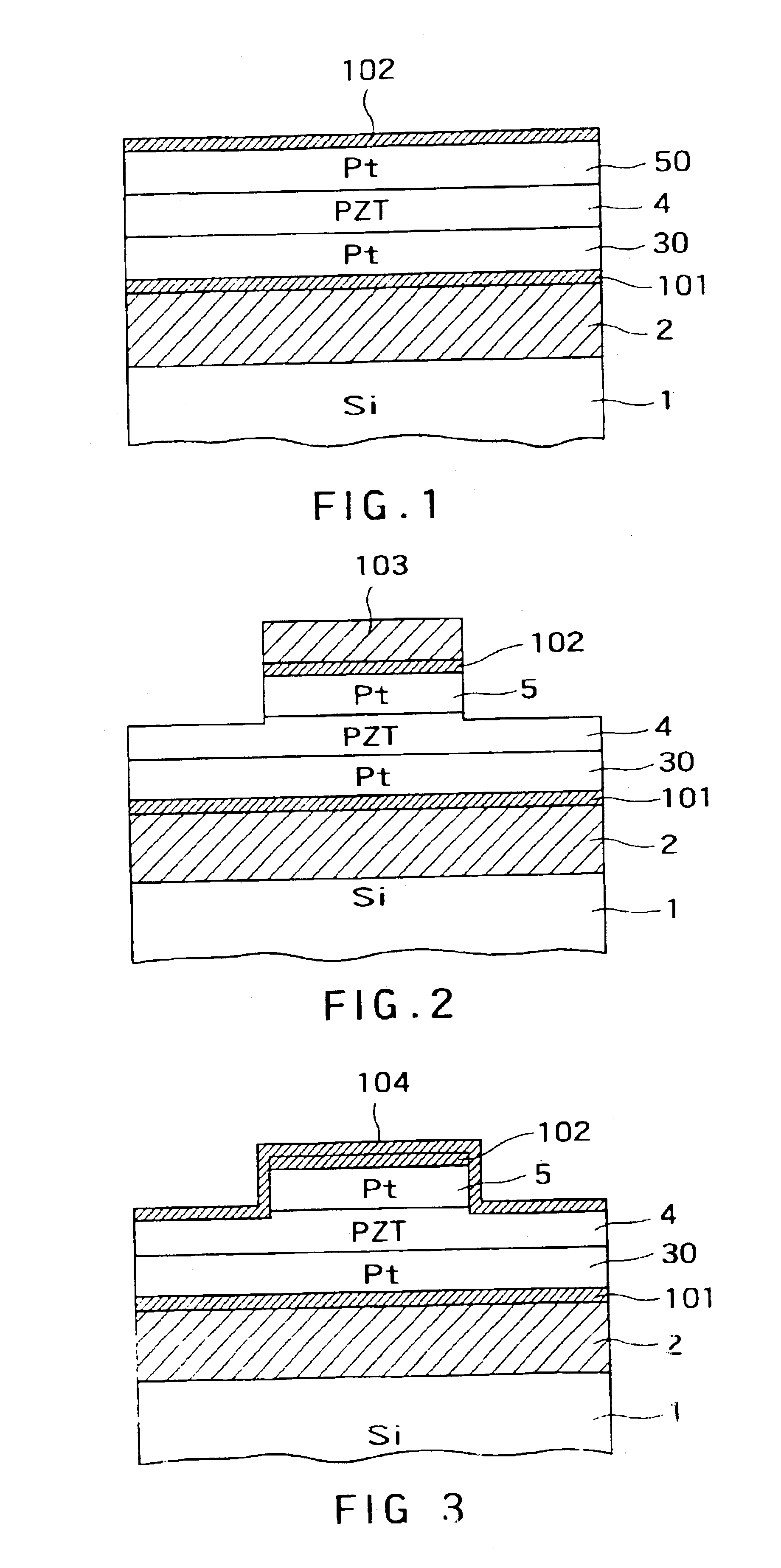
[0103](First Embodiment)

[0104]FIGS. 1 through 5 are cross-sectional views showing a manufacturing process of a ferroelectric capacitor of ferroelectric random access memory according to the first embodiment of the invention. As shown in FIG. 1, after a transistor (not shown) is made on the silicon substrate 1, its surface is covered by an inter-layer insulating film 2 of silicon oxide, for example, to level it. On the inter-layer insulating film 2, an aluminum oxide film (Al2O3 film) 101 is stacked as a hydrogen barrier film commonly used as an adhesion layer by sputtering, for example, to the thickness of about 10 nm, and a lower Pt electrode film 30, approximately 100 nm thick, is stacked thereon by sputtering, for example. On the lower Pt electrode film 30, a PZT film 4, about 150 nm thick, is stacked by sputtering or sol-gel technique, for example. After that, the PZT film 4 is processed by RTA (rapid thermal annealing) in an oxygen atmosphere of 650° C., for example, to crystal...

second embodiment

[0114](Second Embodiment)

[0115]FIGS. 6 through 11 are cross-sectional views showing a manufacturing process of a ferroelectric capacitor of ferroelectric random access memory according to the second embodiment of the invention. In this embodiment, a hydrogen barrier film is made merely on the upper surface of the upper electrode of the ferroelectric capacitor. First as shown in FIG. 6, after a transistor (not shown) is made on the silicon substrate 1, its surface is covered by an inter-layer insulating film 2 of silicon oxide, for example, to level it. On the inter-layer insulating film 2, a lower Pt electrode film 30, approximately 100 nm thick, is stacked thereon by sputtering, for example, via an adhesion layer 201 not containing titanium. On the lower Pt electrode film 30, a PZT film 4, about 150 nm thick, is stacked by sputtering or sol-gel technique, for example. After that, the PZT film 4 is processed by RTA (rapid thermal annealing) in an oxygen atmosphere of 650° C., for ex...

third embodiment

[0122](Third Embodiment)

[0123]FIGS. 12 through 16 are cross-sectional views showing a manufacturing process of a ferroelectric capacitor of ferroelectric random access memory according to the third embodiment of the invention. In this embodiment, a hydrogen barrier film is made to cover and extend over the upper surface, its side surfaces, side surfaces of the ferroelectric film and upper surface of the lower electrode. As shown in FIG. 12, after a transistor (not shown) is made on the silicon substrate 1, its surface is covered by an inter-layer insulating film 2 of silicon oxide, for example, to level it. On the inter-layer insulating film 2, a lower Pt electrode film 30, approximately 100 nm thick, is stacked thereon by sputtering, for example, via an adhesion layer 301 not containing titanium. On the lower Pt electrode film 30, a PZT film 4, about 150 nm thick, is stacked by sputtering or sol-gel technique, for example. After that, the PZT film 4 is processed by RTA (rapid therm...


PUM


Abstract

A semiconductor device having a semiconductor substrate; an insulating film formed on said semiconductor substrate; a ferroelectric capacitor having a lower electrode, a ferroelectric film and an upper electrode which are stacked sequentially on the insulating film; a first hydrogen barrier film; a first inter-layer insulating film covering said ferroelectric capacitor; and a second inter-layer insulating film stacked on the first inter-layer insulating film, the first hydrogen barrier film being interposed between the first and second interlayer insulating films is proposed.

Description

[0001]This is a divisional of application Ser. No. 09 / 570,026 filed May 12, 2000 now U.S. Pat. No. 6,611,014, the contents of which are incorporated herein by reference in their entirety.BACKGROUND OF THE INVENTION[0002]This invention relates to a semiconductor device having a ferroelectric capacitor and its manufacturing method.[0003]For years, there are known non-volatile ferroelectric memory for non-volatile storage of data by using spontaneous polarization of a ferroelectric capacitor. Ferroelectric random access memory is usable without a battery and operable at a high speed, its development to non-touch cards (radio frequency identification, herein after abbreviated RF-ID) is going to start, and its use in replacement of existing SRAM (static random access memory), DRAM (dynamic random access memory), flash memory, etc. and also as memory integrated with logic circuit, is hopefully expected.[0004]A ferroelectric capacitor is typically made by using platinum (Pt) as upper and l...

Claims


Application Information

Patent Timeline
IPC IPC(8): H01L27/11G01C11/22H01L21/02H01L21/8246H01L27/115
CPCH01L27/11502H01L28/55H01L27/11507H10B53/30H10B53/00
Inventor KANAYA, HIROYUKIMORIMOTO, TOYOTAHIDAKA, OSAMUKUMURA, YOSHINORIKUNISHIMA, IWAOIWAMOTO, TSUYOSHI
Owner KK TOSHIBA
Why Eureka
Try Eureka