Light emitting device and method for manufacturing the same
Active Publication Date: 2006-01-31
SEMICON ENERGY LAB CO LTD
View PDF83 Cites 82 Cited by
Summary
Abstract
Description
Claims
Application Information
AI Technical Summary
This helps you quickly interpret patents by identifying the three key elements:
Problems solved by technology
Method used
Benefits of technology
Benefits of technology
[0012]For solving the above problems, an object of the present invention is to provide a method for manufacturing an active-matrix type light emitting device and the configuration of such an active-matrix type light emitting device having high reliability.
[0018]According to the configuration of the light emitting device of the first aspect of the present invention, the surface of the organic insulation film becomes flat, so that the surface of the first electrode also becomes flat, preventing the EL element from occurring short. As the inorganic insulation film is formed, it becomes possible to protect the TFT by blocking the dispersion of impurities form the EL element and prevent the escape of gas from the organic insulation film. Furthermore, as the inorganic insulation film is provided, the organic insulation film is prevented from etching at the time of etching the first electrode. Furthermore, as the inorganic insulation film has a curved surface with a curvature radius, the coverage of the source electrode or the drain electrode becomes excellent. Moreover, the etchingprocessing is performed several times to form steps on the side surface of the inorganic insulation film and the side surface of the organic insulation film at the opening of the interlayer insulation film. Thus, the TFT can be prevented from being damaged at the time of forming a contact hole. As the curve surface with a curvature radius is provided on the insulating material that covers the first electrode, the coverage of the EL layer becomes excellent to inhibit the generation of shrinkage or the like.
[0024]According to the configuration of the light emitting device of the second aspect of the resent invention, the surface of the organic insulation film becomes flat, so that the surface of the first electrode also becomes flat, preventing the EL element from occurring short. In addition, the inorganic insulation film is formed on a place near the active layer of the TFT to effectively protect the TFT by blocking the dispersion of impurities from the EL element. In this case, furthermore, the inorganic insulation film for dispersing hydrogen atoms and the inorganic insulation film for blocking the dispersion of impurities from the EL element are laminated while being in contact with each other.
[0039]In the above third and fours aspects of the present invention, furthermore, the insulating material that covers the end portion of the first electrode may have a curved surface with a curvature radius on an upper end portion thereof, and the curvature radius may be 0.2 μm to 3 μm. As the curved surface having a curvature radius is formed on the upper end portion of the insulating material that covers the end portion of the first electrode, the surface of the first electrode is able to prevent the foreign substance (dust or the like) from being remained at the foot of the first electrode at the time of washing the surface of the first electrode.
Problems solved by technology
In particular, the development of such a transistor has been hurried for providing a switching element of an image displaying device.
The light emitting element having an organic compound has a disadvantage in that it tends to be deteriorated by various factors, so that the greatest problem thereof is to increase its reliability (make longer its life span).
Method used
Image
Click on the blue label to locate the original text in one second.
Reading with bidirectional positioning of images and text.
Examples
example 1
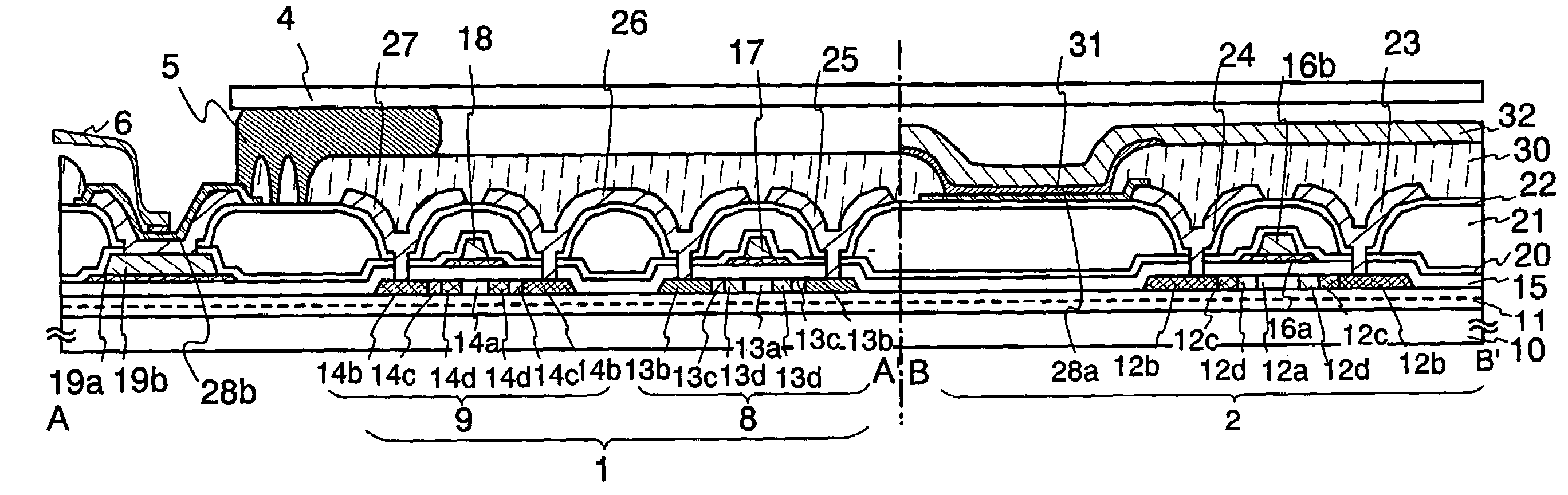
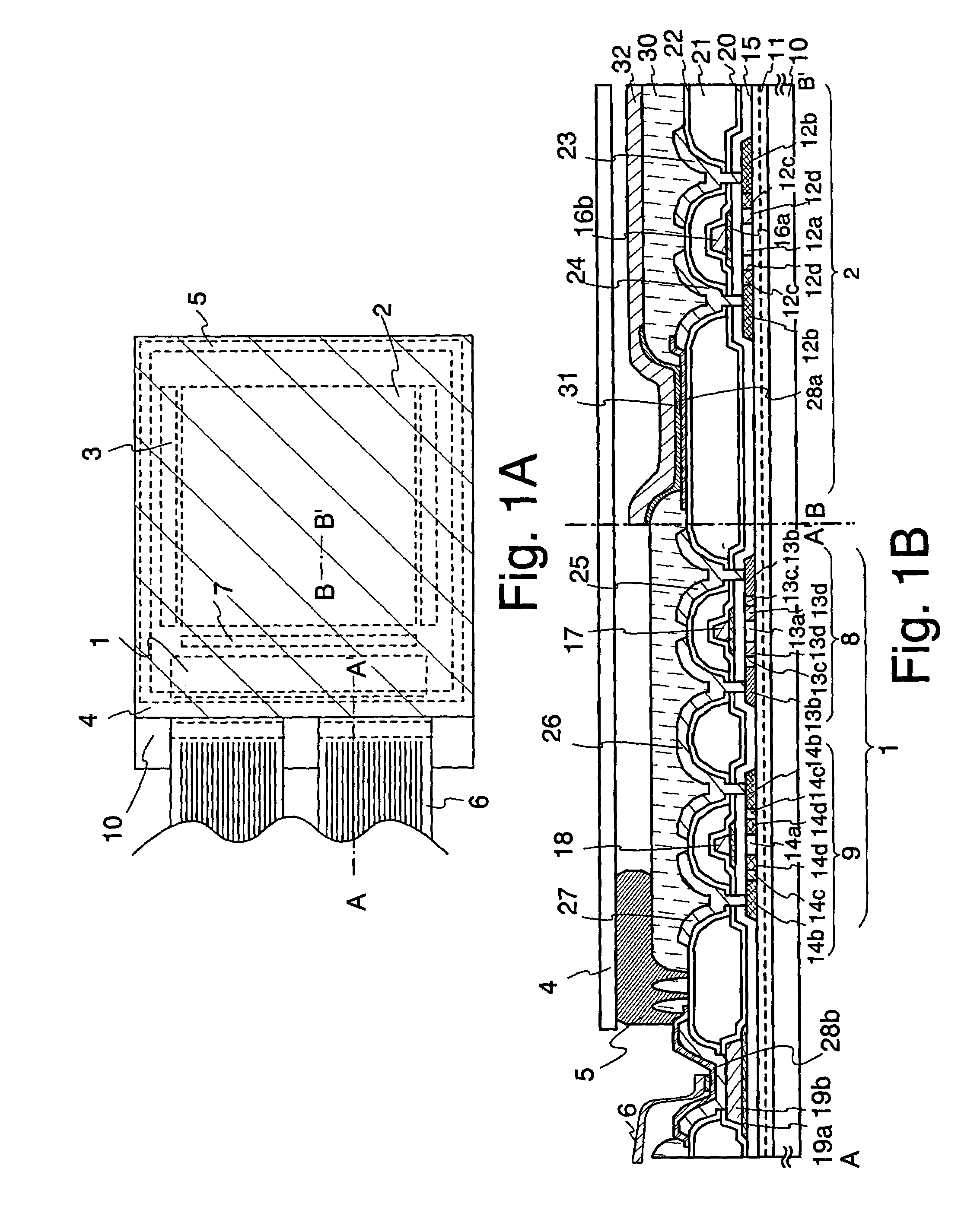
[0138]Here, a method of simultaneously manufacturing a pixel portion, and TFTs (n-channel TFTs and a p-channel TFT) of a driving circuit provided in the periphery of the pixel portion on the same substrate to manufacture the light emitting device having EL element is described in detail using FIGS. 1B and 2.
[0139]For a lower layer of a base insulating film 11, a silicon oxynitride film formed from SiH4, NH3, and N2O as material gases (composition ratio: Si=32%, O=27%, N=24%, H=17%) is formed on the heat resistance glass substrate (the first substrate 10) having a thickness of 0.7 mm with a thickness of 50 nm (preferably 10 to 200 nm) and at a film deposition temperature of 400° C. by using plasma CVD. Then, after the surface is cleaned with ozone water, an oxide film on the surface is removed by means of dilute hydrofluoric acid (dilution with 1 / 100). Next, for an upper layer of the base insulating film 11, a siliconhydride oxynitride film formed from SiH4 and N2O as material gases...
example 2
[0197]In Example 1, there was described an example in which the interlayer insulation film having the curved surface on its upper end portion and the insulating material were formed. In this example, another example which is different from Example 1 is shown in FIGS. 4A and 4B. In FIGS. 4A and FIG. 4B, the same structural components as those of FIG. 1B are represented by the same reference numerals.
[0198]In the present example, there is shown an example in which, after the formation of an interlayer insulation film, a contact hole is formed by etching using the same mask.
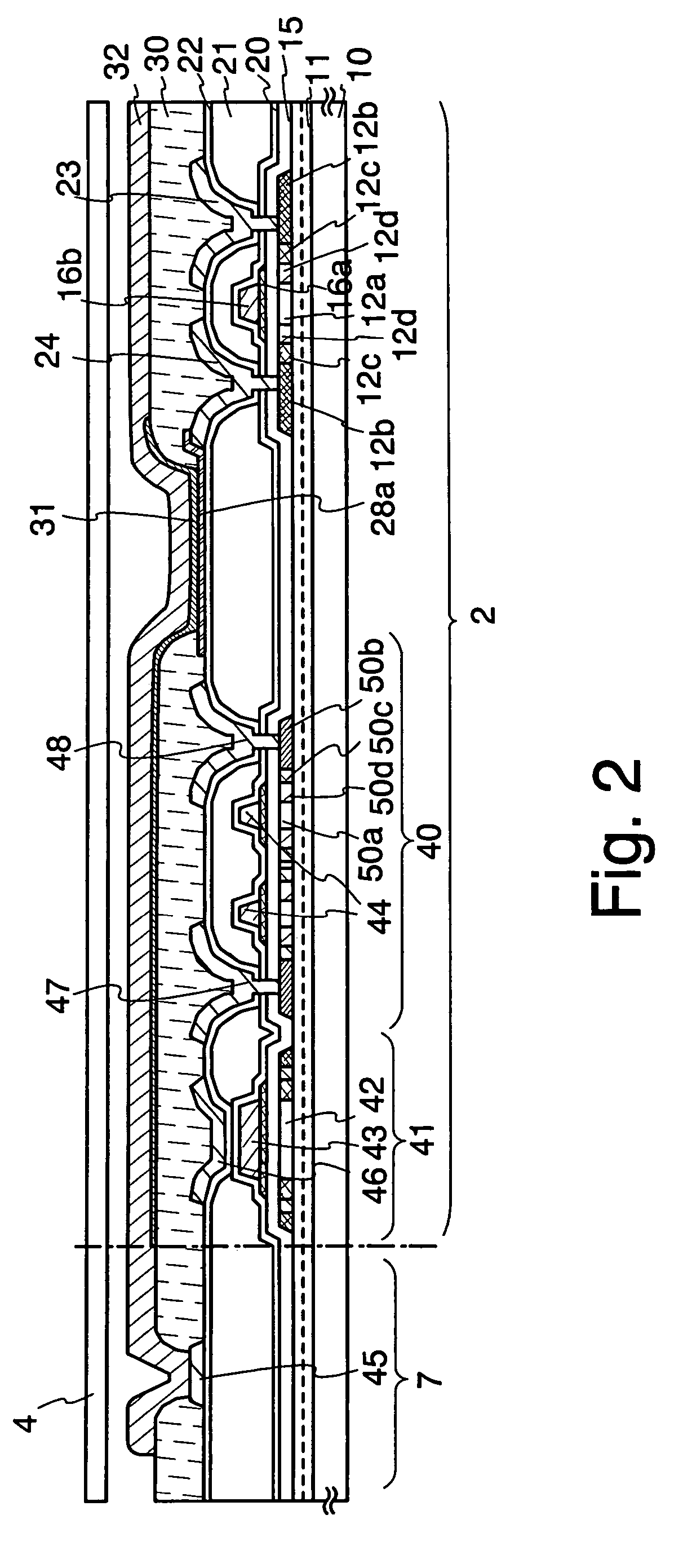
[0203]In this example, as shown in FIG. 6A, the sequence of forming the first electrode, the contact hole, and the connecting electrode is different from that of Example 1. The structure shown in FIG. 6A is provided for illustrating the process by which a CMP processing for flattening the first electrode can be easily performed. However, at the time of patterning for forming a connecting electrode in contact with the first electrode, etching or washing may be preferably performed such that the remainder of etching is prevented from being remained on the first electrode. For simplification, only a point different from Example 1 will be described. Here, in FIG. 6A, the same structural components as those of FIG. 1B are represented by the same reference numerals.
[0204]At first, according to Example 1, a contact hole is formed in each of interlayer insulation films 20, 21, 22, followed by forming a first electrode 628a. Then, a connecting electrode 624 and wiring 23 to 27 are formed suc...
PUM
Abstract
A light emitting element containing an organic compound has a disadvantage in that it tends to be deteriorated by various factors, so that the greatest problem thereof is to increase its reliability (make longer its life span). The present invention provides a method for manufacturing an active matrix type light emitting device and the configuration of such an active matrix type light emitting device having high reliability. In the method, a contact hole extending to a source region or a drain region is formed, and then an interlayer insulation film made of a photosensitive organic insulating material is formed on an interlayer insulation film. The interlayer insulation film has a curved surface on its upper end portion. Subsequently, an interlayer insulation film provided as a siliconnitride film having a film thickness of 20 to 50 nm is formed by a sputtering method using RF power supply.
Description
BACKGROUND OF THE INVENTION[0001]1. Field of the Invention[0002]The present invention relates to a light emitting device using a light emitting element having a layer that contains an organic compound between a pair of electrodes (hereinafter, referred to as a layer containing an organic compound), on which an electric field is applied to obtain fluorescence or phosphorescence, and to a method for manufacturing such a novel light emitting device. Here, the term “light emitting device” used in the present specification represents one of image display devices, light emitting devices, and optical sources (including lighting units). In addition, the light emitting device may be any kind of the light emitting devices, such as a module on which a flexible printed circuit (FPC), a tape automate bonding (TAB), or a tape carrier package (TCP) is attached; a module where a print-wiring plate is mounted on the tip of a TAB tape or TCP; and a module on which an integrated circuit (IC) is direct...
Claims
Application Information
Patent Timeline
Application Date:The date an application was filed.
Publication Date:The date a patent or application was officially published.
First Publication Date:The earliest publication date of a patent with the same application number.
Issue Date:Publication date of the patent grant document.
PCT Entry Date:The Entry date of PCT National Phase.
Estimated Expiry Date:The statutory expiry date of a patent right according to the Patent Law, and it is the longest term of protection that the patent right can achieve without the termination of the patent right due to other reasons(Term extension factor has been taken into account ).
Invalid Date:Actual expiry date is based on effective date or publication date of legal transaction data of invalid patent.

