Method and apparatus for film deposition

a film forming and film technology, applied in chemical vapor deposition coatings, coatings, metallic material coating processes, etc., can solve the problems of damage and short circuit of transistors, film forming methods, and ultraviolet damage, and achieve high utilization efficiency of reaction gas, efficient deposited, and high forming speed

Inactive Publication Date: 2006-03-14
SONY CORP
View PDF29 Cites 25 Cited by
  • Summary
  • Abstract
  • Description
  • Claims
  • Application Information

AI Technical Summary

Benefits of technology

[0015]In view of the foregoing status of the art, it is an object of the present invention to provide a film forming method which controls the kinetic energy of reactive species (deposition species and their precursors) and radical ions like silicon ions of high energy or radical hydrogen ions while utilizing the advantages of the above-described catalyzed CVD method, thereby enabling improvement in tight contact between a produced film and a substrate, improvement in the density of the produced film, improvement in the forming speed, improvement in the smoothness of the produced film, improvement in the burying property into a via-hole and the step coverage, further lowering of the temperature of the substrate, and stress control for the produced film without damaging the substrate, and thus enabling a film of high quality, and a film forming apparatus used for this method.

Problems solved by technology

These film forming methods have problems as follows.
(1) Lack of uniformity and fluctuation of a plasma field, and a non-uniform electric field in plasma-induced electric charges are generated. These may cause damages and short circuits t the transistor (e.g., charge-up or discharge breakdown of a gate oxide film, discharge between wirings, and the like). Particularly, such phenomenon tends to occur at the time of switching on / off the plasma.
(2) There is a possibility of ultraviolet damage due to light emission from the plasma.
(3) Plasma discharge is difficult in a large area, and occurrence of a standing wave makes it difficult to realize uniformity.
(4) The device is complicated and expensive and requires complicated maintenance work.
In the case of the ICB method, too, since cluster ions are led onto the substrate through an aperture of an accelerating electrode so as to collide with the substrate, it is difficult to realize uniformity and to form a film of a large area, that is, a film on a large substrate.
Although this proves that the catalyzed CVD method is a simple method, particularly the momentum of deposition species can only be controlled in accordance with the kinetic theory of gases.
Therefore, it is difficult to use a plastic film substrate having a poor heat resistance property and the degree of freedom in selection of the substrate material is limited.
Also, since the control of the momentum of deposition species is insufficient, burying of a metal for connection into a via-hole (through-hole for connection between wirings) having a particularly large aspect ratio and the step coverage tend to be insufficient.

Method used


Image

  • Method and apparatus for film deposition
  • Method and apparatus for film deposition
  • Method and apparatus for film deposition

Examples


first embodiment

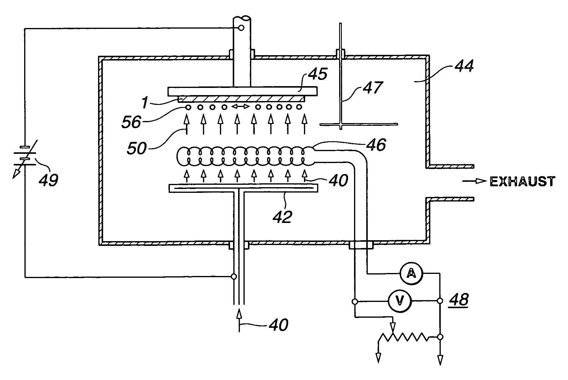
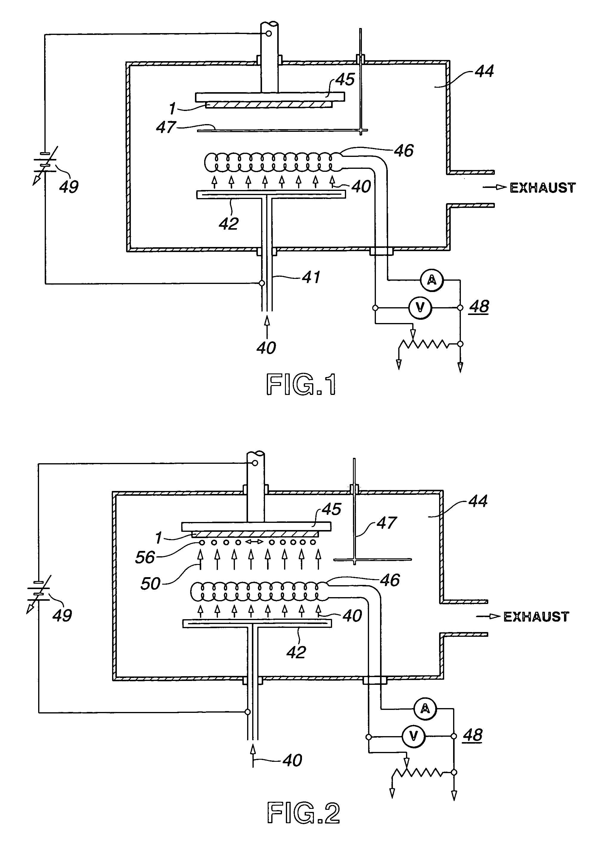
[0086]A first embodiment of the present invention will be described with reference to FIGS. 1 to 10.

[0087]In the present embodiment, on the basis of the catalyzed CVD method, a reaction gas, made of a hydrogen-based carrier gas and a material gas such as a silane gas or the like, is brought in contact with a heated catalyzer made of tungsten or the like, and an electric field of not higher than a glow discharge starting voltage is caused to act on the radical deposition species or its precursor thus produced and radical hydrogen ions, thus providing kinetic energy. Thus, a predetermined film of polycrystal silicon or the like is formed by vapor growth on a substrate. In this case, a DC voltage not higher than the glow discharge starting voltage, that is, a DC voltage determined by the Paschen's law, for example, a voltage not higher than 1 kV is applied between the substrate and a counter-electrode, thus directing the radical deposition species or its precursor and radical hydrogen ...

second embodiment

[0133]A second embodiment of the present invention will now be described with reference to FIG. 7.

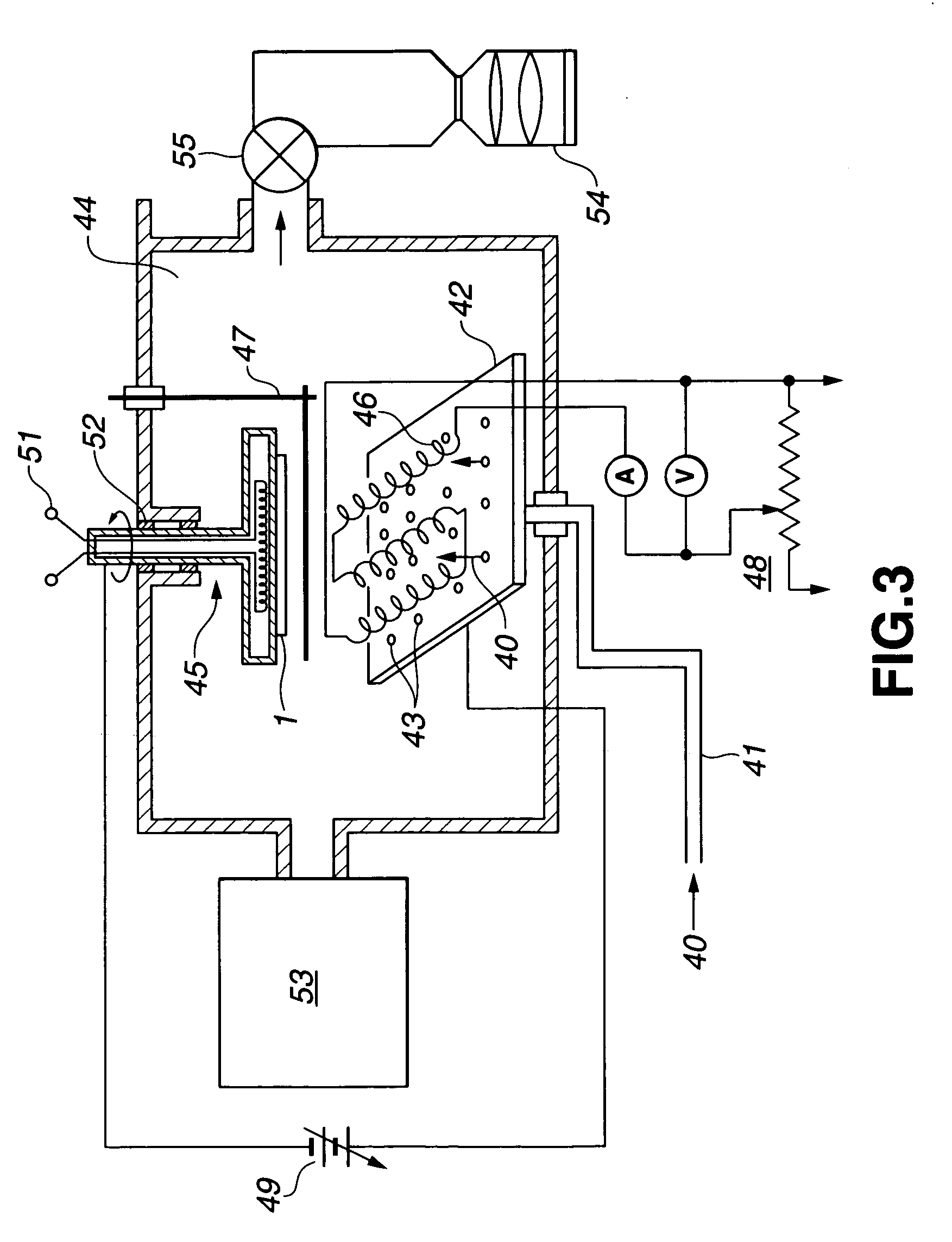
[0134]In the present embodiment, using the DC-bias catalyzed CVD method and the device therefor of the first embodiment, charged particles or ions are provided, that is, an electron shower 100 is provided near a substrate 1 or a suscepter 45 as shown in FIG. 7. Therefore, in addition to the effect of the first embodiment, an excellent effect can be realized as follows.

[0135]At the time of or during the formation of the above-described polycrystal silicon film, radical deposition species of high energy or their precursors and ions might be generated in the reaction gas due to catalytic action of a catalyzer 46, and charge up the substrate 1, thus causing unevenness in the film formation and deterioration in the performance of the film or device. However, by irradiating the ions and the like with electrons having directionality and concentration due to a DC field from the electron shower ...

third embodiment

[0136]A third embodiment of the present invention will now be described with reference to FIG. 8.

[0137]In the present embodiment, a mesh electrode 101 for accelerating reactive species is provided between a substrate 1 and a catalyzer 46 as shown in FIG. 8, in the DC-bias catalyzed CVD method and the device therefor of the first embodiment.

[0138]Specifically, a plurality of mesh electrodes 101a and 101b having gas passage holes 101c are provided between the substrate 1 and the catalyzer 46, and a DC voltage 49 not higher than 1 kV is applied between them, thereby providing kinetic energy in the direction toward the substrate 1 to the reactive species generated by decomposition of the reaction gas due to the catalyzer 46 as described above. Therefore, in addition to the effect similar to that of the first embodiment, an accelerating electrode which is designed and processed in advance can be easily inserted as the mesh electrode 101 into the gap between the substrate 1 and the cataly...


PUM

PropertyMeasurementUnit
frequencyaaaaaaaaaa
temperatureaaaaaaaaaa

Abstract

A reaction gas made of a hydrogen-based carrier gas and a silane gas or the like is brought in contact with a heated catalyzer of tungsten or the like, and a DC voltage not higher than a glow discharge starting voltage or a voltage produced by superimposing an AV voltage or an RF voltage on the DC voltage is applied on the produced reactive species, so as to provide kinetic energy and carry out vapor growth of a predetermined film on a substrate, thereby providing a film of high quality.

Description

TECHNICAL FIELD[0001]This invention relates to a film forming method and a film forming apparatus for vapor growth of a predetermined film made of polycrystal silicon or the like.BACKGROUND ART[0002]Conventionally, a chemical vapor deposition (CVD) method for a polycrystal silicon layer has been used in manufacturing a metal-insulator-semiconductor field effect transistor (MISFET), for example, a MIS thin film transistor (MISTFT), in which a polycrystal silicon layer formed on a substrate is used as source, drain and channel regions.[0003]In the case of forming a polycrystal silicon layer of this type by the ordinary CVD method, reactive species which are produced by decomposition of a material gas in a vapor phase reach the substrate and react on the substrate, thereby forming a film. Alternatively, the reactive species react in a region very close to the surface of the substrate and are deposited thereon. In order for the film to be produced and epitaxially grow, the reactive spec...

Claims


Application Information

Patent Timeline
Patent Type & Authority Patents(United States)
IPC IPC(8): C23C16/00C23C16/24C23C16/34C23C16/40C23C16/44C23C16/503C23C16/509H01L21/205
CPCC23C16/24C23C16/345C23C16/402C23C16/44H01L21/02658C23C16/5096H01L21/02422H01L21/02532H01L21/0262C23C16/503
Inventor YAMANAKA, HIDEOKAISE, KIKUO
Owner SONY CORP
Why Eureka
Try Eureka