
Method to restore hydrophobicity in dielectric films and materials

a technology of applied in the field of restoration of hydrophobicity in dielectric films and materials, can solve the problems of increasing power consumption and signal cross-talk, interconnection rc delay, undesirable properties,

Inactive Publication Date: 2006-04-18
HONEYWELL INT INC
View PDF7 Cites 43 Cited by
  • Summary
  • Abstract
  • Description
  • Claims
  • Application Information

AI Technical Summary

Benefits of technology

The invention provides a method for producing nanoporous silica dielectric films with a low dielectric constant (“k”) and improved hydrophobicity. The method involves contacting the damaged silica dielectric film with a surface modification composition and removing unreacted surface modification composition. The surface modification composition includes at least one surface modification agent, such as a compound or charged derivative thereof, suitable for removing silanol moieties from the damaged silica dielectric film. The methods can be applied to both nanoporous and non-porous silica dielectric films. The surface modification composition can also include a solvent. The technical effects of the invention include improved adhesion, reduced damage to the substrate, and improved reliability of the semiconductor or IC device.

Problems solved by technology

As feature sizes in integrated circuits approach 0.25 μm and below, problems with interconnect RC delay, power consumption and signal cross-talk have become increasingly difficult to resolve.
Undesirable properties result when the silica-based materials, such as the nanoporous silica dielectric films mentioned herein, form nanoporous films with surfaces, including surfaces of the pore structures, that contain silanol groups.
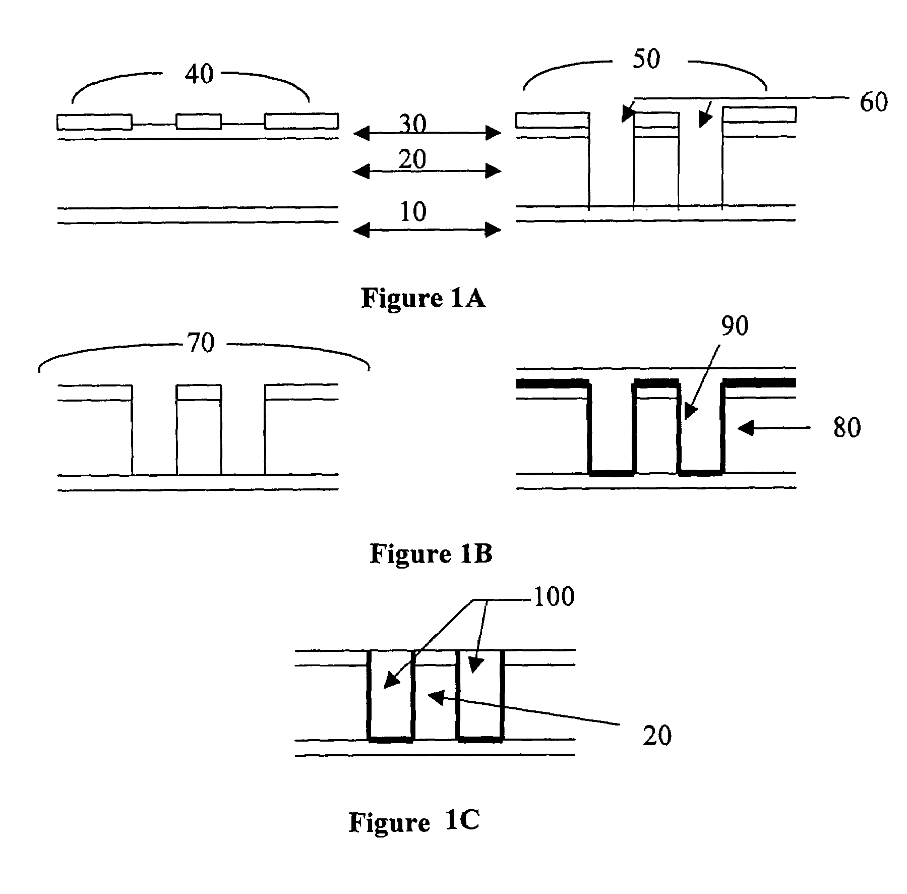
Damage to nanoprous silica dielectric films during during semiconductor manufacturing processes results from the application of aggressive plasmas and / or etching reagents to etch trenches and vias into dielectric films.
Dielectric films which are exposed to these plasmas during trench, via, etch and / or photoresist removal are easily degraded or damaged.
Porous dielectric films have a very high surface area and are therefore particularly vulnerable to plasmas damage.
The chemicals used are often so aggressive they will attack and remove organic groups in silica based dielectric films, especially porous silica films.
Again, this damage will cause the films to lose their hydrophobicity.

Method used


Image

  • Method to restore hydrophobicity in dielectric films and materials
  • Method to restore hydrophobicity in dielectric films and materials

Examples


example 1

Formation of Nanoporous Silica Film Treated with MTAS

[0064]A nanoporous silica precursor was synthesized as described by co-owned U.S. Ser. No. 09 / 235,186, filed on Jan. 22, 1999, incorporated by reference herein. Thus, the precursor was prepared by adding 208 mL of tetraethoxysilane, 94 mL of triethyleneglycol monomethyl ether(TriEGMME), 16.8 mL deionized water, and 0.68 mL of 1N nitric acid together in a round bottom flask. The solution was allowed to mix vigorously and heated (heating and stirring were begun at the same time) to about 80° C. and refluxed for 1.5 hours, to form a clear solution. The resulting solution was allowed to cool down to room temperature and then it was diluted 25% by weight with ethanol, and filtered through a 0.1 micron Teflon® filter.

[0065]About 2 mL of the nanoporous silica precursor was deposited onto a 4″ silicon wafer and then spun at 2500 rpm for 30 seconds. Then the film was gelled / aged in a vacuum chamber using the following conditions:[0066]1. T...

example 2

Formation of Non-Porous Methylhydridosiloxane Film

[0075]A precursor composition was prepared as described by U.S. patent application Ser. No. 09 / 044,798, filed on Mar. 20, 1998, the disclosure of which is incorporated by reference herein. Thus, a one liter jacketed reactor equipped with a nitrogen inlet, dry ice condenser and a mechanical stirrer was charged with 1000 mL hexanes, 80 mL ethanol, 25 mL water and 61.3 g Amberjet 4200 catalyst (Rohn & Haas Co.). The mixture was equilibrated for 0.5 hr with stirring at 25° C. (circulating bath). A mixture of trichlorosilane (14.3 mL, 0.142 Mol) and methyltrichlorosilane (66.7 mL, 0.568 Mol) was added to the reactor using a peristaltic pump over a period of 35 minutes. Upon completion of the silane addition, hexane was pumped through the lines for 10 minutes. The reaction was stirred for 23 hours, then filtered through a Whatman #4 filter. The filtered solution was placed in a separatory funnel and the water / ethanol layer removed. The rem...

example 3

Photoresist Ashing

[0078]The wafer coated with nanoporous silica in Example 1 is placed within the chamber of a TEL 85 DRM L3510 etcher. Pure oxygen is made to flow through the chamber at less than 500 sccm. The wafer temperature is 25° C. An RF plasma source is activated at a power consumption level of 500 W for a period of 1 minute. During this 1 minute period the film is exposed to a plasma derived from oxygen. The total pressure during this process is less than 500 millitorr. The predicted film properties before and after this ashing treatment are:

[0079]

TABLE 2ThicknessRIkC—H Abs.Before7050 Å1.1652.20.15After69601.1603.80.02

[0080]Fourier transform infrared (“FTIR”) spectroscopy confirms that the O—H absorption curve is increased in amplitude at about 3500 cm−1 in films subjected to the ashing treatment, relative to untreated (non-ashed) films. This confirms that the ashing treatment removes most of the C—H bonds attributable to the methyl groups in the original film. It has previ...


PUM

PropertyMeasurementUnit
feature sizesaaaaaaaaaa
dielectric constantsaaaaaaaaaa
dielectric constantaaaaaaaaaa

Abstract

Silica dielectric films, whether nanoporous foamed silica dielectrics or nonporous silica dielectrics are readily damaged by fabrication methods and reagents that reduce or remove hydrophobic properties from the dielectric surface. The invention provides for methods of imparting hydrophobic properties to such damaged silica dielectric films present on a substrate. The invention also provides plasma-based methods for imparting hydrophobicity to both new and damaged silica dielectric films. Semiconductor devices prepared by the inventive processes are also provided.

Description

CROSS REFERENCE TO RELATED APPLICATION[0001]This application claims the benefit of Provisional patent application Ser. No. 60 / 214,219 filed Jun. 23,2000.FIELD OF THE INVENTION[0002]The invention provides methods and compositions for restoring hydrophobicity to the surfaces of silica dielectric films. These films are used as insulating materials in the manufacture of semiconductor devices such as integrated circuits (“ICs”) in order to ensure low and stable dielectric properties in these films.BACKGROUND OF THE INVENTION[0003]As feature sizes in integrated circuits approach 0.25 μm and below, problems with interconnect RC delay, power consumption and signal cross-talk have become increasingly difficult to resolve. It is believed that the integration of low dielectric constant materials for interlevel dielectric (ILD) and intermetal dielectric (IMD) applications will help to solve these problems. While there have been previous efforts to apply low dielectric constant materials to inte...

Claims


Application Information

Patent Timeline
Patent Type & Authority Patents(United States)
IPC IPC(8): G03C5/56B08B7/00B32B3/10G03F7/16G03F7/40H01L21/02H01L21/3105H01L21/312H01L21/316H01L21/768
CPCH01L21/02063H01L21/02203H01L21/02216H01L21/02282H01L21/02304H01L21/02337H01L21/0234H01L21/02343H01L21/02359H01L21/02362H01L21/3105H01L21/31058H01L21/3122H01L21/31695H01L21/76814H01L21/7682H01L21/76826H01L21/76831H01L21/02126Y10T428/24802H01L21/31
Inventor HACKER, NIGEL P.THOMAS, MICHAELDRAGE, JAMES S.
Owner HONEYWELL INT INC
Learn More