On chip power supply

a technology of integrated circuit and power supply, which is applied in the direction of electronic switching, pulse technique, instruments, etc., can solve the problems of requiring careful timing control, reducing the attractiveness reducing the efficiency of external power utilization, so as to achieve a more conductive “, reduce leakage, and improve the effect of gate driv

Inactive Publication Date: 2006-04-18
ARRAY OPTRONIX
View PDF15 Cites 5 Cited by
  • Summary
  • Abstract
  • Description
  • Claims
  • Application Information

AI Technical Summary

Benefits of technology

[0018]During the “on” state of these IC's, the power supply will provide power to drive the control circuits which can be used to generate a more conductive “on” state, and a lower leakage “off” state. In the case of an ICD, the forward voltage can be significantly reduced, to a level equivalent to or better than that of a synchronous rectifier. In the case of a surface field effect transistor IC, the gate drive can be substantially enhanced, providing a reduced “on resistance” which equates to forward voltage reduction.

Problems solved by technology

Utilizing external power for this purpose tends to be less attractive because of the added circuit board complexity.
However, the same are rarely used, not only because of their incompatibility with silicon integrated circuit fabrication, but because of temperature sensitivity and other undesirable characteristics thereof.
In circuits that utilize the true rectifying characteristics of semiconductor diodes, the forward conduction voltage drop of the diode is usually a substantial disadvantage.
Use of a semiconductor switch to couple the secondary to the output has the advantage of a very low forward conduction voltage drop, and has the disadvantage of requiring careful timing control throughout the operating temperature range of the converter to maintain the efficiency of the energy transfer from primary to secondary.
These circuits are obviously very costly.
The use of a semiconductor diode for this purpose has the advantage of eliminating the need for control of a secondary switch, but has the disadvantage of imposing the forward conduction voltage drop of the semiconductor diode on the secondary circuit.
First, the forward conduction voltage drop of the semiconductor diode device can substantially reduce the efficiency of the converter.
In the case of a 3 volt power supply, the imposition of a 0.7 volt series voltage drop means that the converter is in effect operating into a 3.7 volt load, thereby limiting the efficiency of the converter to 81%, even before other circuit losses are considered.
Second, the efficiency loss described above represents a power loss in the diode, resulting in the heating thereof.
This limits the power conversion capability of an integrated circuit converter, and in many applications requires the use of a discrete diode with a heat sink of adequate size, increasing the overall circuit size and cost.
Here two diode voltage drops are imposed on the peak DC output, making the circuit particularly inefficient using conventional diodes, and increasing the heat generation of the circuit requiring dissipation through large discrete devices, heat dissipating structures, etc. depending on the DC power to be provided.
Further, while reverse current leakage is always undesirable and normally must be made up by additional forward conduction current, thereby decreasing circuit efficiency, reverse current leakage can have other and more substantial deleterious affects on some circuits.
They also provide an attractive alternative for the higher voltage portion of the synchronous rectifier market; however, they are not able to replace the entire synchronous rectifier market.

Method used


Image

  • On chip power supply
  • On chip power supply
  • On chip power supply

Examples


Embodiment Construction

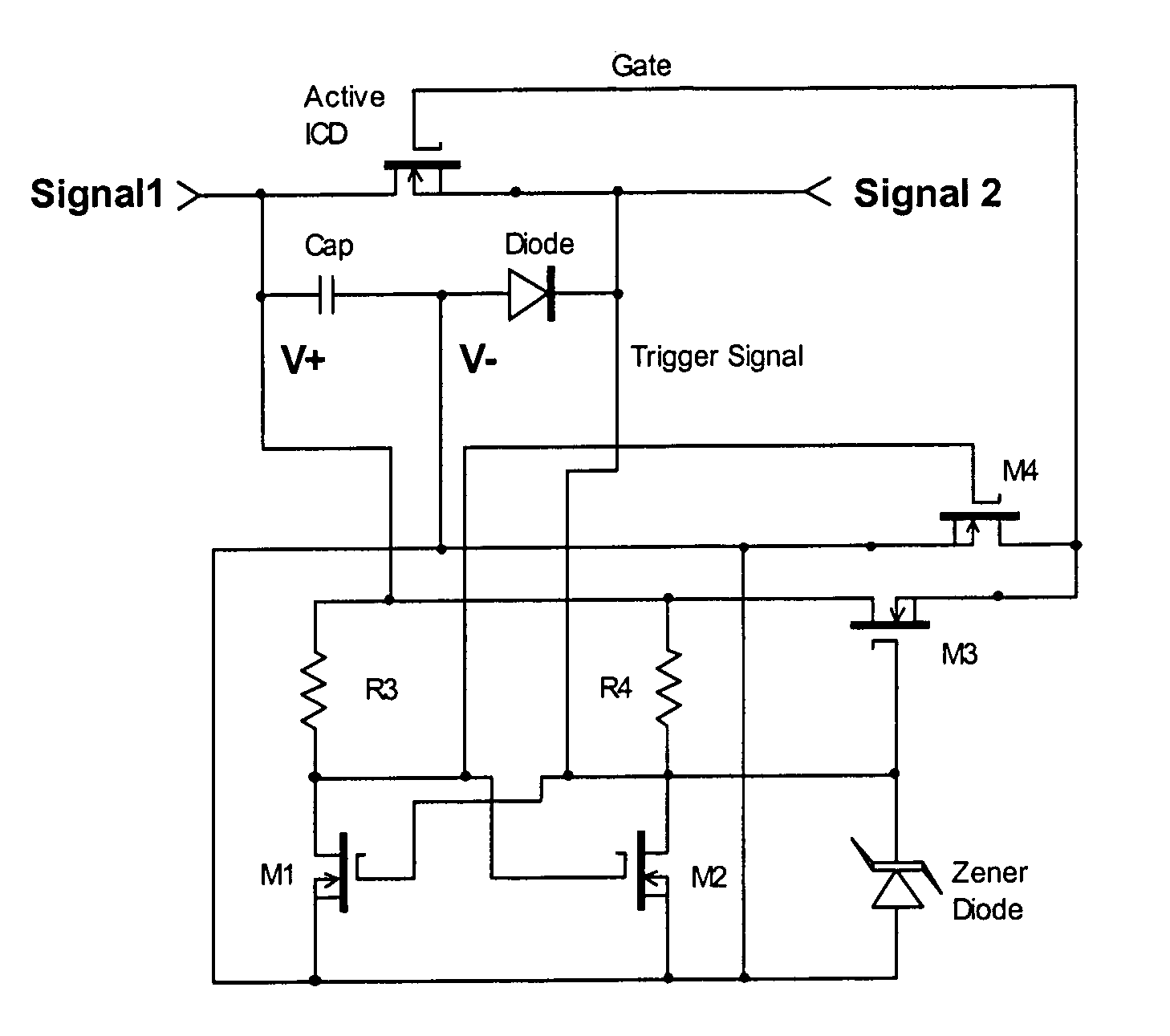
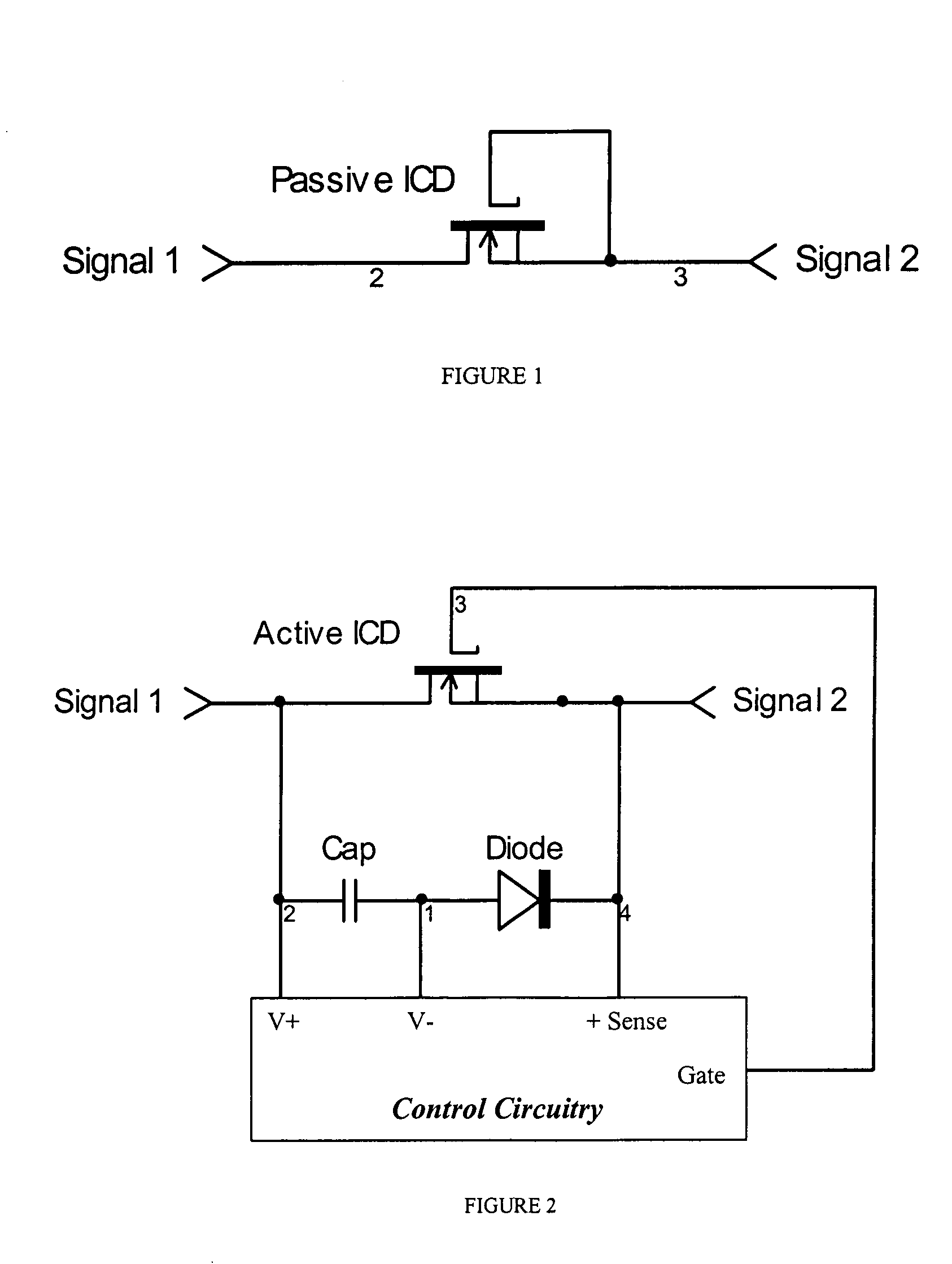
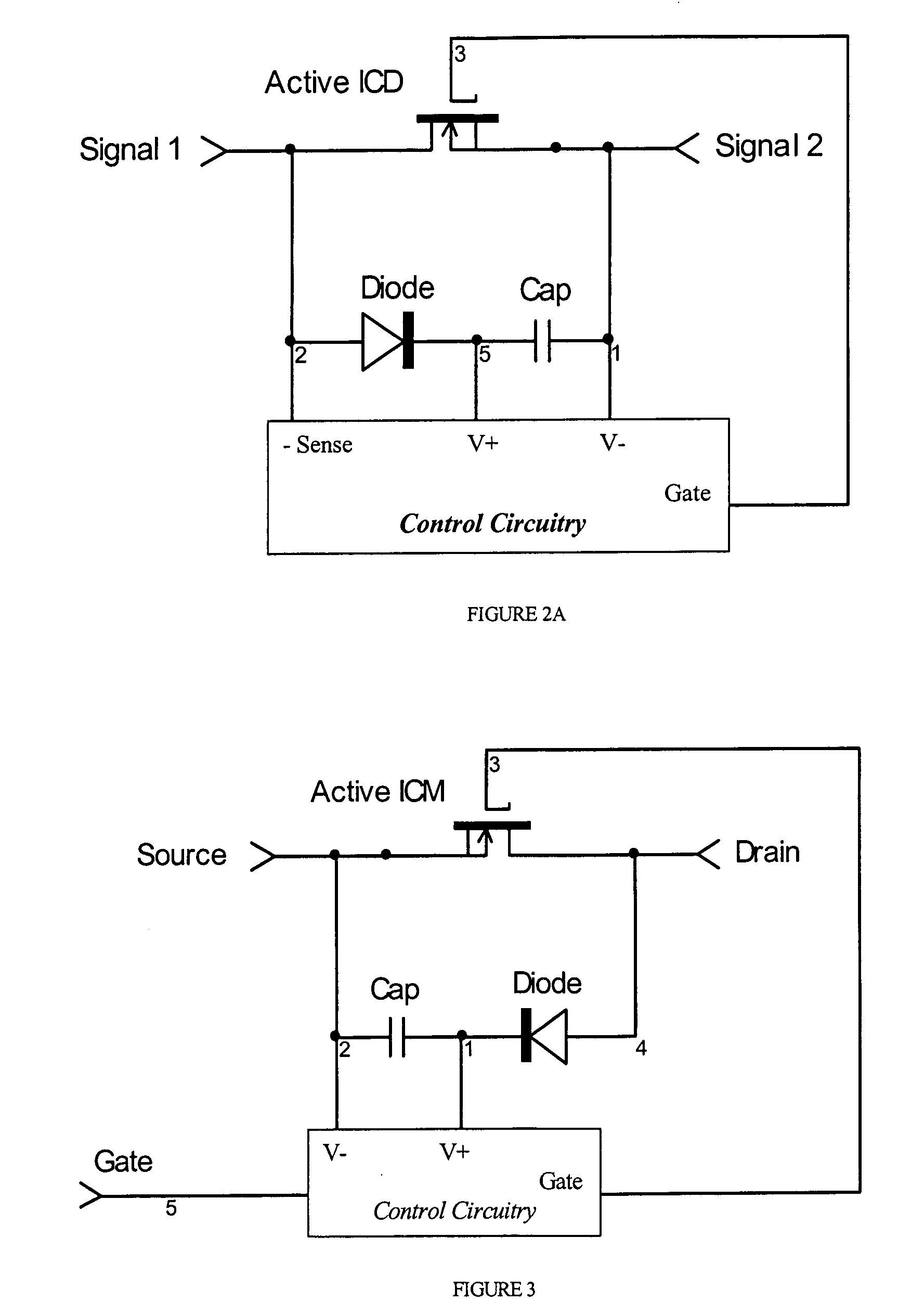
[0026]Referring to FIG. 1, a prior art schematic diagram of an ICD (integrated circuit diode) is presented. This device acts as a low forward voltage diode because of the gate connections, and the depletion threshold voltage. It is specifically designed to handle alternating polarities. It is obvious that the addition of an external power supply and control logic would greatly enhance the functionality of this device by allowing the gate to be driven well above the drain potential when conducting.

[0027]The device shown in FIG. 1 is an n-channel device. Normally, in a conventional field effect device, the body or backgate is connected to the source of the charge carriers when the device is turned on. In that regard, the source and drain labels, as used herein refer to the source being that region which is the source of the charge carriers when the device is turned on or conducting, and with the drain being the other region of the same conductivity type. Therefore, the charge carriers...


PUM


Abstract

A technique, for drawing power from the external signal circuit to power on-chip elements for an integrated circuit diode (ICD), utilizes an integrated diode and capacitor. The capacitor is charged by the external applied voltage during the time the ICD blocks the external current flow. The charged capacitor then acts as a battery to power the on-chip circuits to provide active control for the ICD function. This ICD could be provided as a two terminal discrete diode, or integrated onto a larger IC. This same technique can be utilized for a “self powered” MOSFET IC (ICM), utilizing a low power logic signal to trigger an internal circuit which would provide a much larger gate drive than the logic signal could provide. This could also be provided as discrete three terminal components, or integrated into a larger IC.

Description

CROSS-REFERENCE TO RELATED APPLICATION[0001]This application claims the benefit of U.S. Provisional Patent Application No. 60 / 451,060 filed Feb. 26, 2003.BACKGROUND OF THE INVENTION[0002]1. Field of the Invention[0003]The present invention relates to integrated circuit semiconductor diodes and transistors.[0004]2. Prior Art[0005]Semiconductor devices tend to be divided into discrete components and integrated circuits. The discrete devices include single function components such as bipolar transistors, junction field effect transistors, surface field effect transistors, silicon controlled rectifiers, etc. and some integrated components such as insulated gate bipolar transistors. One characteristic that is common to all the discrete components is the lack of external power supply requirements.[0006]Recently a new form of discrete circuit has entered the market; a highly efficient diode made from surface field effect transistors, an integrated circuit diode (ICD). This circuit in its p...

Claims


Application Information

Patent Timeline
Patent Type & Authority Patents(United States)
IPC IPC(8): H03K17/687G05F1/565
CPCG05F1/565H03K2217/0081H03K2017/307G05F1/56H01L21/18H01L29/768
Inventor METZLER, RICHARD A.
Owner ARRAY OPTRONIX
Why Eureka
Try Eureka