Method for producing p-type group III nitride compound semiconductor

a nitride compound and semiconductor technology, applied in semiconductor devices, lasers, semiconductor lasers, etc., can solve the problems of increasing the drive voltage and the inability to obtain ohmic junctions in consideration of ohmic contact with metal, so as to reduce resistance and improve the percentage of activated p-type impurities in the first group iii nitride compound semiconductor layer.

Inactive Publication Date: 2006-05-09
TOYODA GOSEI CO LTD
View PDF15 Cites 12 Cited by
  • Summary
  • Abstract
  • Description
  • Claims
  • Application Information

AI Technical Summary

Benefits of technology

[0012]Therefore, an object of the invention is to provide a method for producing low-resistance p-type Group III nitride compound semiconductor equivalent to the GaP or GaAs compound semiconductor by desorbing p-type impurities held in interstitial sites from the inside of crystal efficiently.
[0013]A method of producing low-resistance p-type Group III nitride compound semiconductor according to the invention includes the steps of: forming a first Group III nitride compound semiconductor layer doped with p-type impurities; forming a second Group III nitride compound semiconductor layer substantially not doped with any impurities or substantially doped with n-type impurities or substantially doped with n-type and p-type impurities; and reducing resistance after or during the step of forming the second Group III nitride compound semiconductor layer. Incidentally, the reason why the second Group III nitride compound semiconductor layer is doped with n-type impurities or n-type and p-type impurities is as follows. When the second Group III nitride compound semiconductor layer is doped with n-type impurities, p-type impurities existing in interstitial sites of the first Group III nitride compound semiconductor layer are taken in the second Group III nitride compound semiconductor layer, that is, solubility is increased because n-type impurities functioning as a donor having properties opposite to those of p-type impurities functioning as an acceptor added to the first Group III nitride compound semiconductor layer are added to the second Group III nitride compound semiconductor layer. On the other hand, when the second Group III nitride compound semiconductor layer is doped with n-type and p-type impurities, diffusion of p-type impurities existing in interstitial sites of the first Group III nitride compound semiconductor layer into the second Group III nitride compound semiconductor layer is promoted in addition to the effect due to addition of n-type impurities. Hereupon, “substantially” means that there are no other intentional impurities in the second Group III nitride compound semiconductor layer. Thus, “the second Group III nitride compound semiconductor layer substantially not doped with any impurities” means that there are no intentional impurities in the second Group III nitride compound semiconductor layer.
[0017]As described above, the method of producing low-resistance p-type Group III nitride compound semiconductor according to the invention includes the steps of: forming a first Group III nitride compound semiconductor layer doped with p-type impurities; and forming a second Group III nitride compound semiconductor layer not doped with any impurities or doped with n-type impurities or with n-type and p-type impurities. Accordingly, the difference in p-type impurity concentration is formed between the first Group III nitride compound semiconductor layer and the second Group III nitride compound semiconductor layer, so that p-type impurities existing in interstitial sites of the first Group III nitride compound semiconductor layer are moved to the second Group III nitride compound semiconductor layer by use of such a diffusing phenomenon that p-type impurities are moved from the first Group III nitride compound semiconductor layer high in p-type impurity concentration to the second Group III nitride compound semiconductor layer low in p-type impurity concentration. As a result, p-type impurities are desorbed from the first Group III nitride compound semiconductor layer. The method of producing low-resistance p-type Group III nitride compound semiconductor according to the invention further includes the step of reducing resistance after or during the step of forming the second Group III nitride compound semiconductor layer. Accordingly, the percentage of activated p-type impurities contained in the first Group III nitride compound semiconductor layer can be improved.

Problems solved by technology

If the thickness is larger than 100 nm, there occur a disadvantage that a drive voltage increases when the semiconductor is applied to a device because the second Group III nitride compound semiconductor layer itself is higher in resistivity (i.e., lower in hole carrier density) than the first Group III nitride compound semiconductor layer, and a disadvantage that ohmic junctions cannot be obtained in consideration of ohmic contact with metal.

Method used


Image

  • Method for producing p-type group III nitride compound semiconductor
  • Method for producing p-type group III nitride compound semiconductor

Examples


embodiment 1

[Embodiment 1]

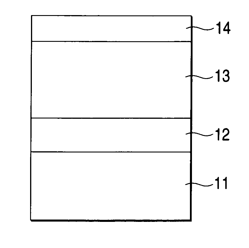
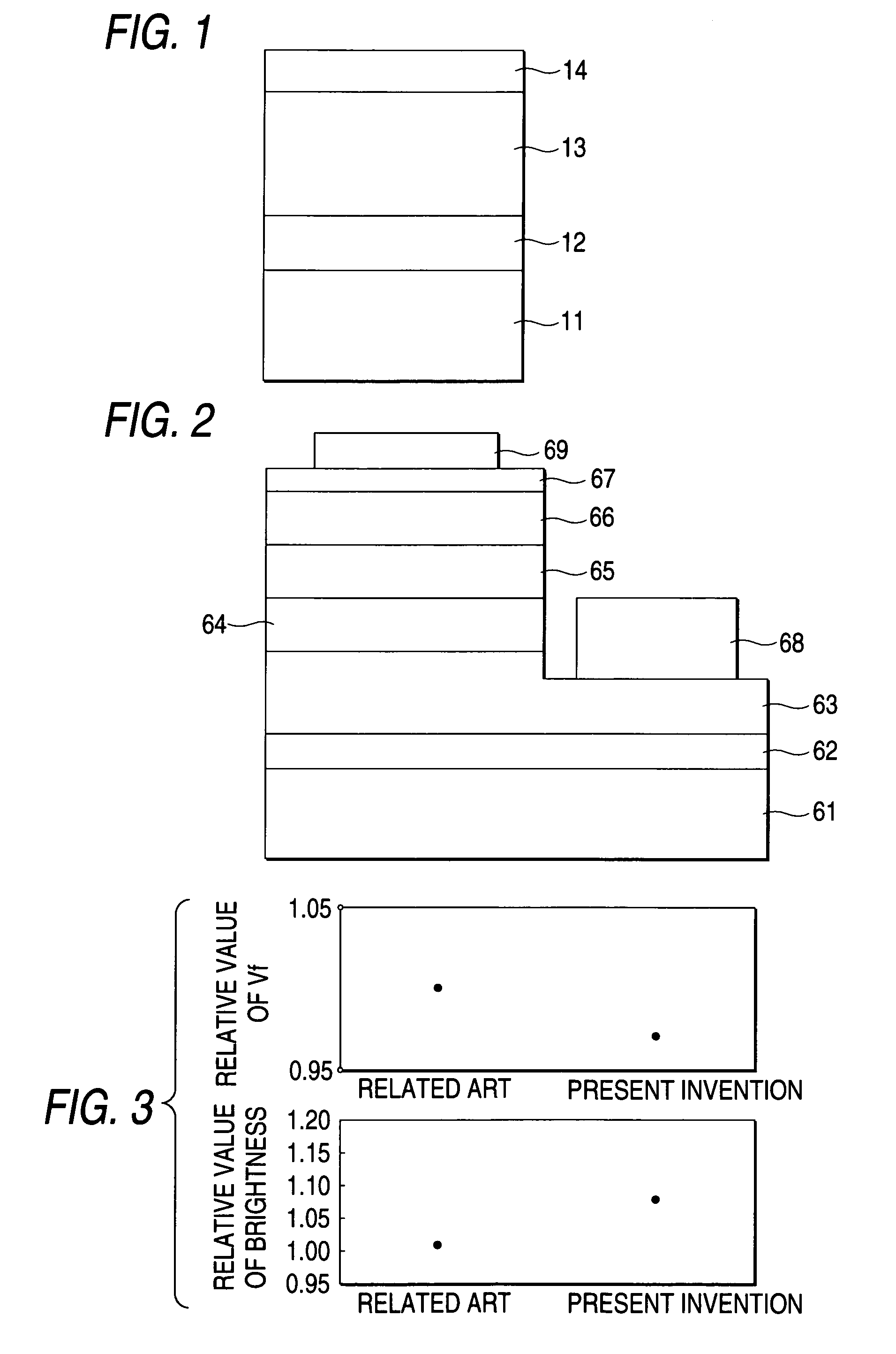
[0027]Embodiment 1 shows the case where impurities are not added to the second Group III nitride compound semiconductor layer. FIG. 1 is a view typically showing the configuration of this embodiment. Specifications of respective layers are as follows.

[0028]

LayerComposition (Impurities)Second Group III nitride compoundGa0.85In0.15Nsemiconductor layer 14First Group III nitride compoundGaN (Mg)semiconductor layer 13Buffer layer 12AlNSubstrate 11sapphire

[0029]First, a sapphire substrate cleaned well was put on a susceptor in an MOVPE apparatus (hereinafter referred to as “reactor”). After the reactor was evaluated to a vacuum, a surface of the sapphire substrate was etched and cleaned at 1050° C. for 20 minutes while a hydrogen gas was made to flow into the reactor. Then, the substrate temperature was decreased to 400° C. and a 30 nm-thick AlN buffer layer was grown on the substrate while a TMA (trimethyl aluminum) gas as an Al source, an ammonia gas as an N source and a h...

embodiment 2

[Embodiment 2]

[0034]Embodiment 2 shows the case where n-type impurities are added to the second Group III nitride compound semiconductor layer. At the time of growth of the Ga0.85In0.15N layer as the second Group III nitride compound semiconductor layer after the growth of the Mg-doped GaN layer as the first Group III nitride compound semiconductor layer in Embodiment 1, an SiH4 (silane) gas was made to flow along with the TMI gas, the TMG gas, the ammonia gas and the nitrogen gas to thereby add Si as n-type impurities to the Ga0.85In0.15N layer.

[0035]Holes in the Mg-doped GaN layer as the first Group III nitride compound semiconductor layer subjected to electron beam irradiation in the same manner as in Embodiment 1 were measured. A result of the measurement was substantially the same as in Embodiment 1 and exhibited very excellent characteristic compared with the related art.

embodiment 3

[Embodiment 3]

[0036]Embodiment 3 shows the case where n-type and p-type impurities are added to the second Group III nitride compound semiconductor layer. At the time of growth of the Ga0.85In0.15N layer as the second Group III nitride compound semiconductor layer after the growth of the Mg-doped GaN layer as the first Group III nitride compound semiconductor layer in Embodiment 1, an SiH4 (silane) gas and a DEZ (diethyl zinc) gas were made to flow along with the TMI gas, the TMG gas, the ammonia gas and the nitrogen gas to thereby simultaneously add Si as n-type impurities and Zn as p-type impurities to the Ga0.85In0.15N layer.

[0037]Holes in the Mg-doped GaN layer as the first Group III nitride compound semiconductor layer subjected to electron beam irradiation in the same manner as in Embodiment 1 were measured. A result of the measurement was substantially the same as in Embodiment land exhibited very excellent p-type characteristic compared with the related art.


PUM

PropertyMeasurementUnit
thicknessaaaaaaaaaa
thicknessaaaaaaaaaa
temperatureaaaaaaaaaa

Abstract

A second Group III nitride compound semiconductor layer not doped with any impurities or doped with n-type impurities or with n-type and p-type impurities is formed on a first Group III nitride compound semiconductor layer doped with p-type impurities. Resistance is reduced by a heat treatment after or during the formation of the second Group III nitride compound semiconductor layer.

Description

[0001]The present application is based on Japanese Patent Applications Nos. 2002-272554 and 2003-279732, which are incorporated herein by reference.BACKGROUND OF THE INVENTION[0002]1. Field of the Invention[0003]The present invention relates to Group III nitride compound semiconductors used in optical devices such as light-emitting diodes in a range of from an ultraviolet region to a red region, laser diodes, etc., and electronic devices such as high-temperature devices, etc. and particularly to methods for producing low-resistance p-type Group III nitride compound semiconductors.[0004]2. Description of the Related Art[0005]Generally, even in the case where p-type impurities are added to a Group III nitride compound semiconductor produced by an metal organic vapor phase epitaxy method (MOVPE method), it is impossible to obtain low-resistance p-type semiconductor crystal as obtained in a gallium phosphide (GaP) or gallium arsenide (GaAs) semiconductor which is a Group III-Group V com...

Claims


Application Information

Patent Timeline
Patent Type & Authority Patents(United States)
IPC IPC(8): H01L21/00H01L21/20H01L21/205H01L21/225H01L21/263H01L21/324H01L33/06H01L33/32H01S5/323
CPCH01L21/0237H01L21/0242H01L21/02458H01L21/0254H01L21/02576H01L21/02579H01L21/2258H01L21/3245H01L33/14H01L21/0262H01S2301/173H01L33/025H01L33/32H01S5/32341
Inventor TAKI, TETSUYA
Owner TOYODA GOSEI CO LTD
Why Eureka
Try Eureka