Electrode, manufacturing method of the same, and dye-sensitized solar cell
a manufacturing method and technology of electrodes, applied in the direction of superimposed coating process, sustainable manufacturing/processing, final product manufacturing, etc., can solve the problems of insufficient amount, inability to achieve sufficient improvement of photoelectric conversion efficiency, and difficulty in employing plastic substrates with poor thermal resistance to glass substrates. achieve high photoelectric conversion efficiency, improve productivity and economical efficiency, and improve the effect of dye replacement properties
- Summary
- Abstract
- Description
- Claims
- Application Information
AI Technical Summary
Benefits of technology
Problems solved by technology
Method used
Image
Examples
first embodiment
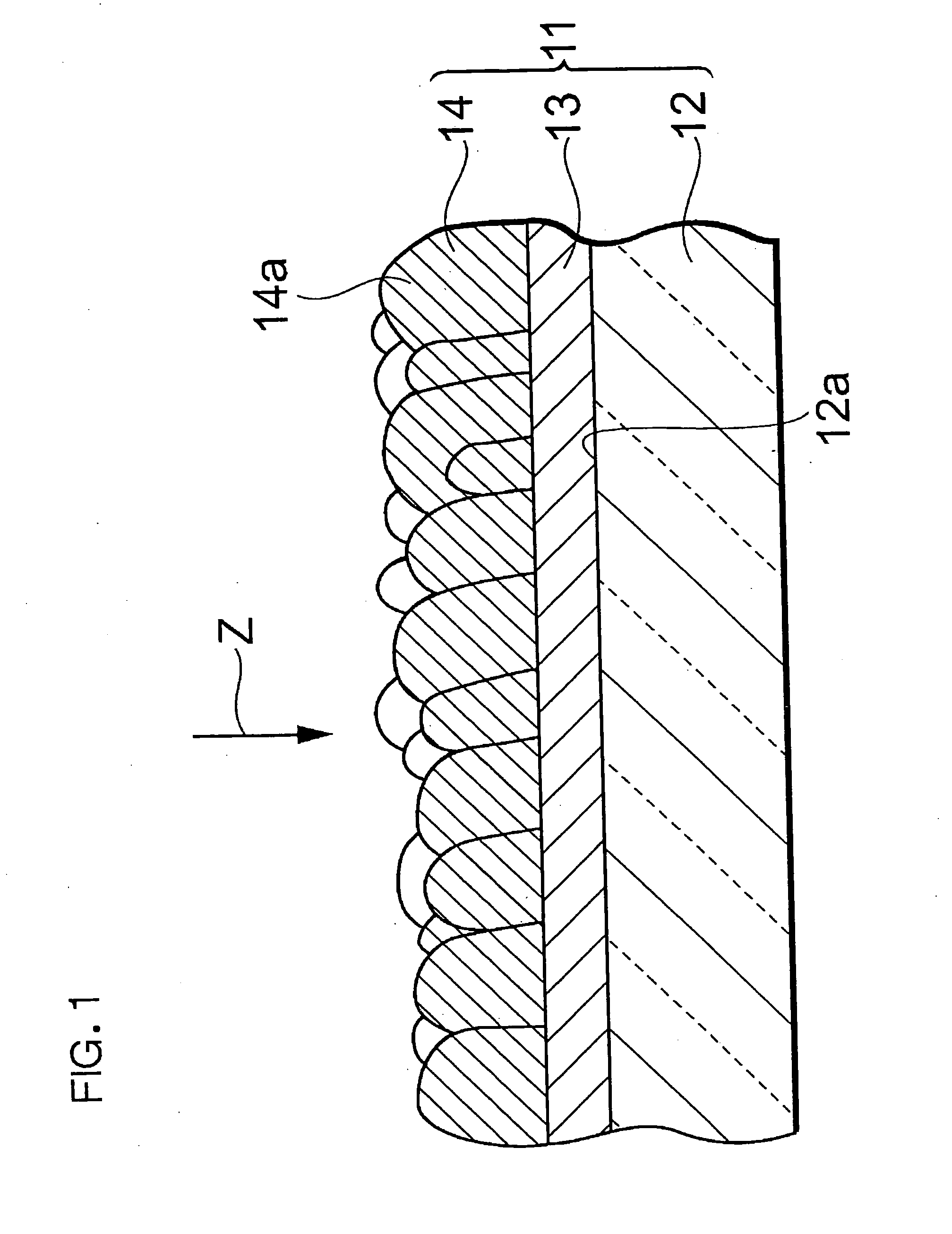
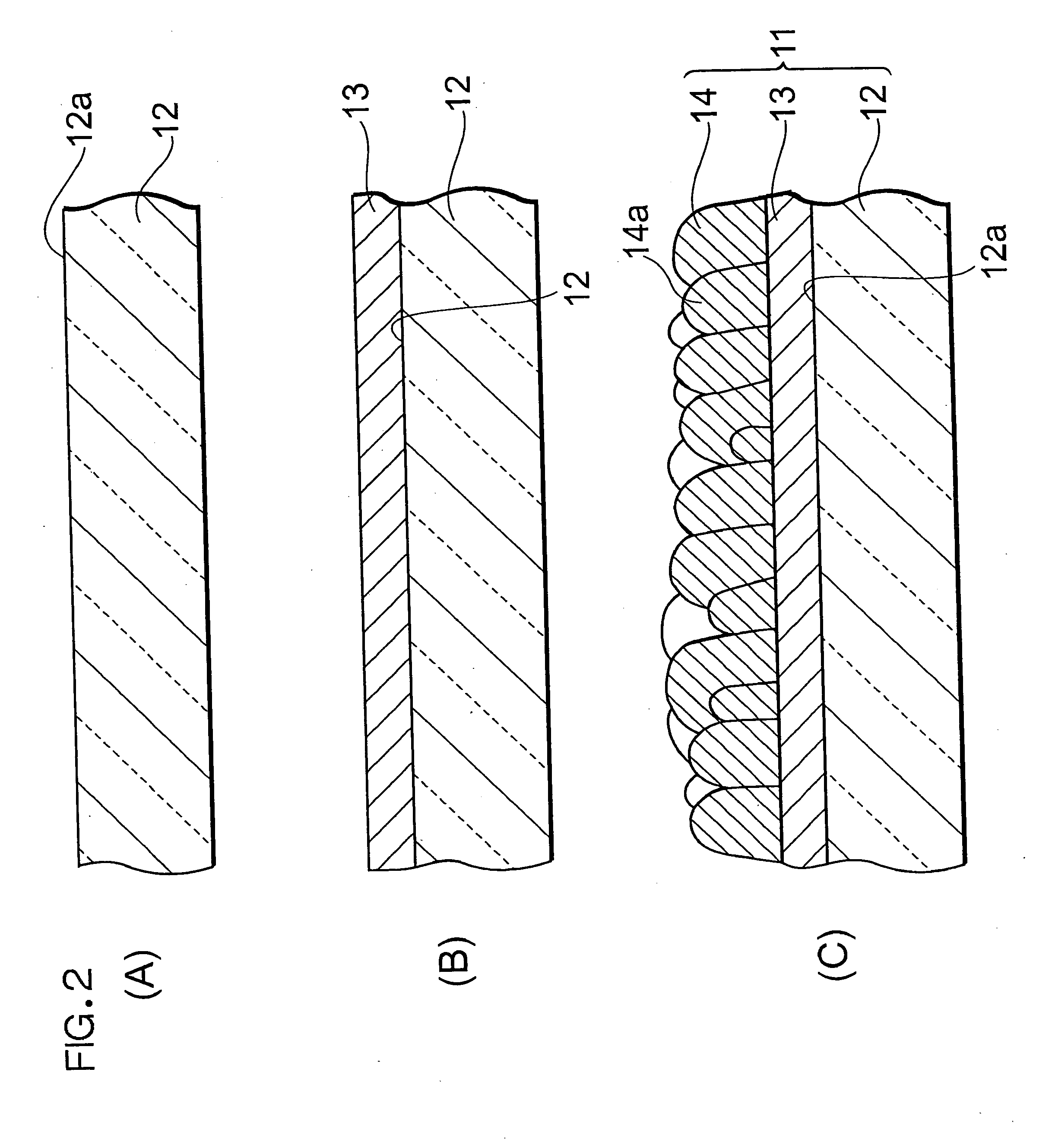
[0037]FIG. 1 is a schematic sectional view schematically showing one embodiment of an electrode according to the present invention. In an electrode 11, a porous dye-supported layer 14 including zinc oxide and a sensitizing dye is laminated on a substrate 12 having a conductive surface 12a. Thus, a metal oxide layer is constituted of the dye-supported layer 14.
[0038]There is not any special restriction on a type or a dimensional shape of the substrate 12 as long as the substrate can support at least the dye-supported layer 14. For example, a plate-like or sheet-like substrate is preferably used. In addition to a glass substrate, examples of the substrate include a plastic substrate of polyethylene terephthalate, polyethylene, polypropylene or polystyrene, a metal substrate, an alloy substrate, a ceramic substrate, and a laminated substrate thereof. The substrate 12 preferably has an optical transparency, and more preferably has an excellent optical transparency in a visible light ran...
second embodiment
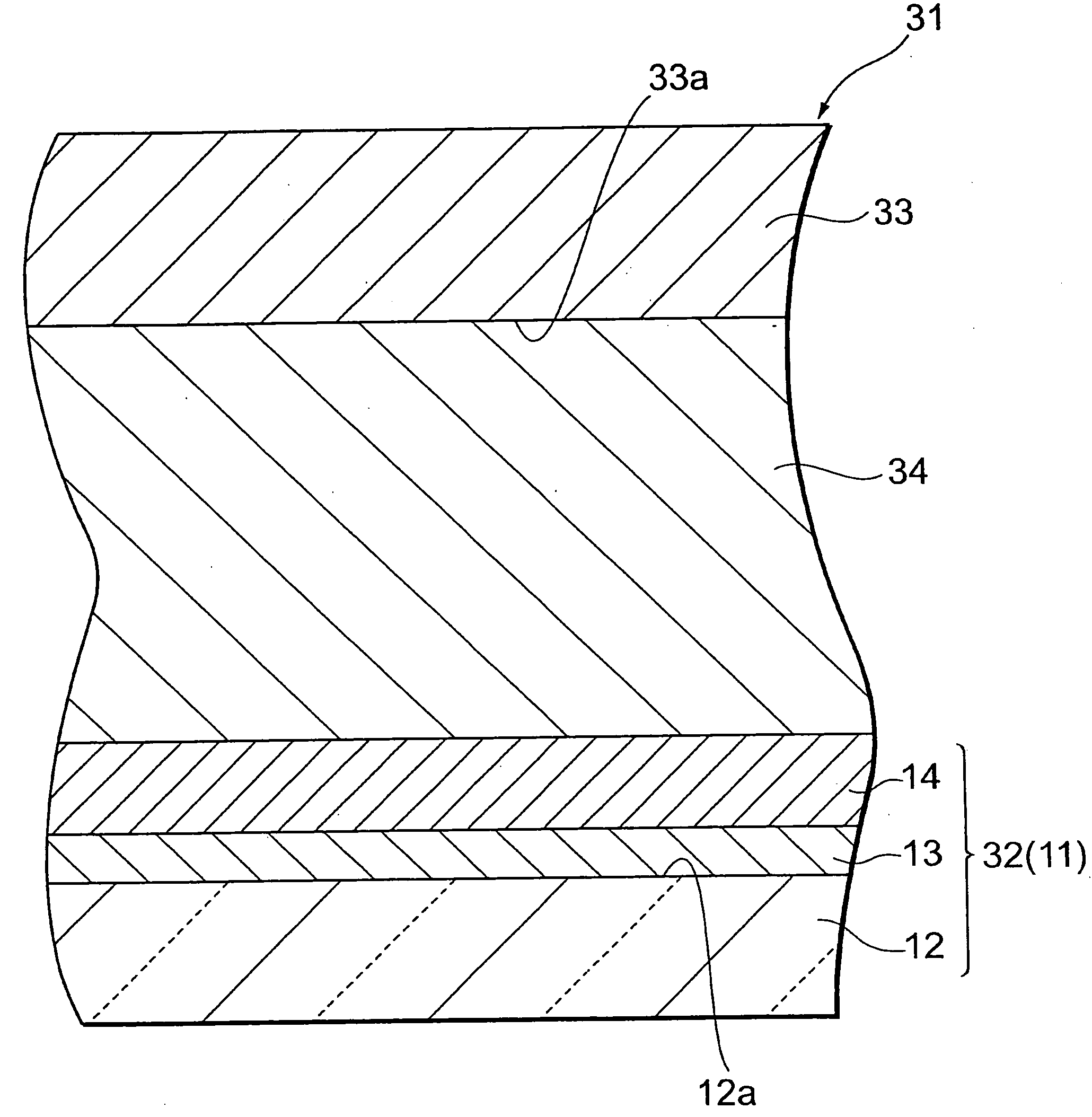
[0071]FIG. 3 is a schematic sectional view schematically showing one embodiment of a solar cell according to the present invention. A dye-sensitized solar cell 31 (the solar cell) includes an electrode 11 described above in the first embodiment, as a photoelectric conversion electrode (element), and has a-photoelectric conversion electrode 32 (the electrode 11), a counter electrode 33 disposed so as to face the electrode 32, and a charge transport layer 34 disposed between the photoelectric conversion electrode 32 and the counter electrode 33.
[0072]The counter electrode 33 is disposed so that a conductive surface 33a of the counter electrode faces a dye-supported layer 14. As the counter electrode 33, a known electrode may appropriately be employed. For example, in the same manner as in a substrate 12 of the electrode 11 having a conductive surface 12a, there may be used an electrode having a conductive film on a transparent substrate, an electrode in which a film of a metal, carbon...
examples
[0075]The present invention will hereinafter be described in detail with respect to examples, but the present invention is not limited to these examples.
PUM
| Property | Measurement | Unit |
|---|---|---|
| Molar density | aaaaa | aaaaa |
| Electric potential / voltage | aaaaa | aaaaa |
| Efficiency | aaaaa | aaaaa |
Abstract
Description
Claims
Application Information


