Methods of fabricating silicon carbide metal-semiconductor field effect transistors

a metal-semiconductor field effect transistor and silicon carbide technology, applied in the field of microelectronic devices, can solve the problems of limited power handling capability of previously known jfets, high power and high frequency transistors usually generate larger amounts of heat, and achieve the effect of reducing back-gate effects and improving performan

Inactive Publication Date: 2006-06-27
CREE INC
View PDF60 Cites 24 Cited by
  • Summary
  • Abstract
  • Description
  • Claims
  • Application Information

AI Technical Summary

Benefits of technology

[0015]Embodiments of the present invention may provide SiC MESFETs formed on a semi-insulating substrate of SiC where the SiC substrate is substantially free of deep level dopants. Forming SiC MESFETs on such semi-insulating substrates may improve performance by reducing back-gating effects which may result from the presence of deep level dopants in the substrate. Buffer layers of p-type, n-type or undoped SiC may be utilized with such semi-insulating SiC substrates in the formation of MESFETs according to embodiments of the present invention.

Problems solved by technology

Previously, bipolar transistors and power metal-oxide semiconductor field effect transistors (MOSFETs) have been used for high power applications but the power handling capability of such devices may be limited at higher operating frequencies.
Junction field-effect transistors (JFETs) were commonly used for high frequency applications but the power handling capability of previously known JFETs also may be limited.
In turn, high power and high frequency transistors usually generate larger amounts of heat than small signal transistors.
Although these devices provided increased operating frequencies and moderately increased power handling capability, the relatively low breakdown voltage and the lower thermal conductivity of these materials have limited their usefulness in high power applications.
Unfortunately, difficulty in manufacturing has limited the usefulness of SiC for high power and high frequency applications.
Although the SiC on Si substrate devices described in U.S. Pat. Nos. 4,762,806 and 4,757,028 may have exhibited improved thermal characteristics, the use of a Si substrate generally limits the ability of such devices to dissipate heat.
Furthermore, the growth of SiC on Si generally results in defects in the epitaxial layers which result in high leakage current when the device is in operation.

Method used


Image

  • Methods of fabricating silicon carbide metal-semiconductor field effect transistors
  • Methods of fabricating silicon carbide metal-semiconductor field effect transistors
  • Methods of fabricating silicon carbide metal-semiconductor field effect transistors

Examples


first embodiment

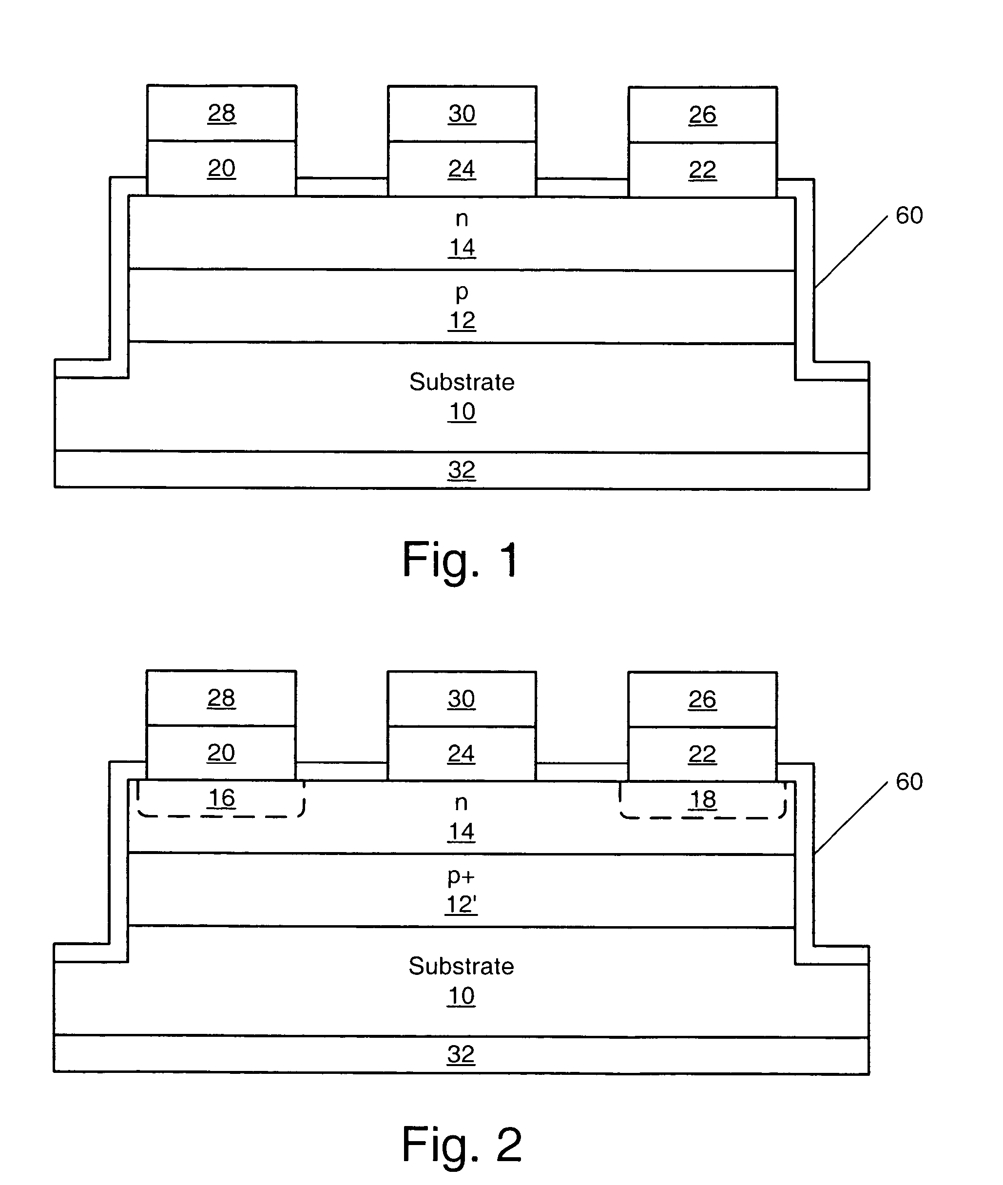
[0061]FIG. 1 illustrates a MESFET of the present invention. A first epitaxial layer 12 of p-type conductivity is grown on a single crystal bulk silicon carbide substrate 10 of either p-type or n-type conductivity or semi-insulating. The first epitaxial layer of silicon carbide 12 is disposed between the substrate 10 and an n-type epitaxial layer 14. An optional metallization layer, 32 may be formed on the opposite side of the substrate from the first epitaxial layer 12. The metallization layer 32 is preferably formed as described below with reference to FIG. 5.

[0062]The first epitaxial layer 12 may be a p-type conductivity silicon carbide epitaxial layer, an undoped silicon carbide epitaxial layer or a very low doped n-type conductivity silicon carbide epitaxial layer. If a low dope silicon carbide epitaxial layer is utilized, then it is preferred that the doping concentration of the first epitaxial layer 12 be less than about 5×1015 cm−3. If an undoped or n-type first epitaxial lay...

second embodiment

[0065]FIG. 2 illustrates a MESFET according to the present invention. As seen in FIG. 2, a selectively doped p-type epitaxial layer 12′ is formed on the substrate 10. The second n-type epitaxial layer 14 is formed on the selectively doped first p-type epitaxial layer 12′ and the source and drain contacts 20, 22 and Schottky metal contact 24 are formed on the n-type epitaxial layer 14. Also illustrated in FIG. 2 are optional n+ regions 16 and 18 formed in the source and drain regions of the device. If the n+ regions 16 and 18 are formed, it is preferred that these regions be formed by ion implantation of preferably phosphorous (P), although nitrogen (N) may also be used, followed by a high temperature anneal. Suitable anneal temperatures may be from about 1100 to about 1600° C.

[0066]Alternatively, the n+ regions 16 and 18 may be eliminated as described above so as to provide a device having the source, drain and gate structure illustrated in FIG. 1. In such a case, it is preferred th...

third embodiment

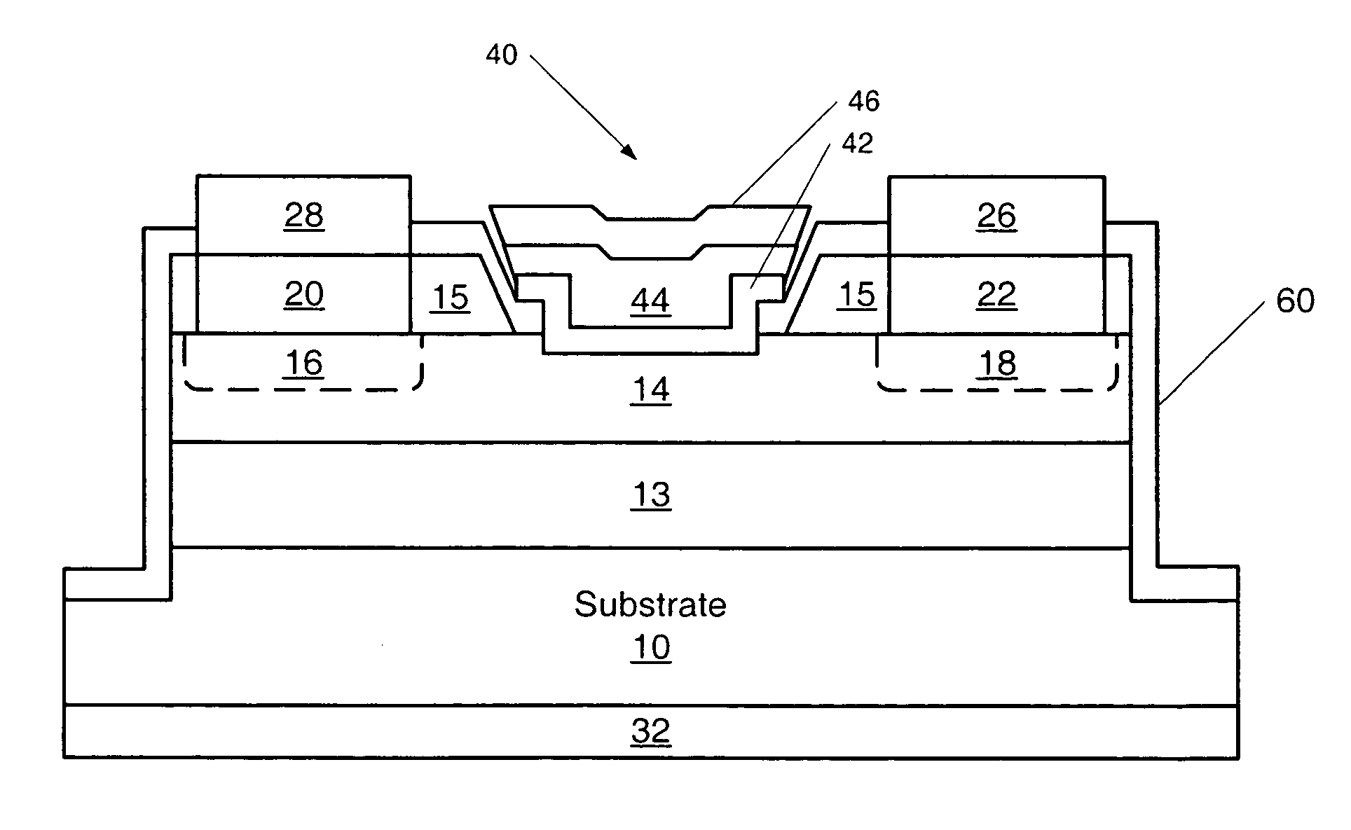
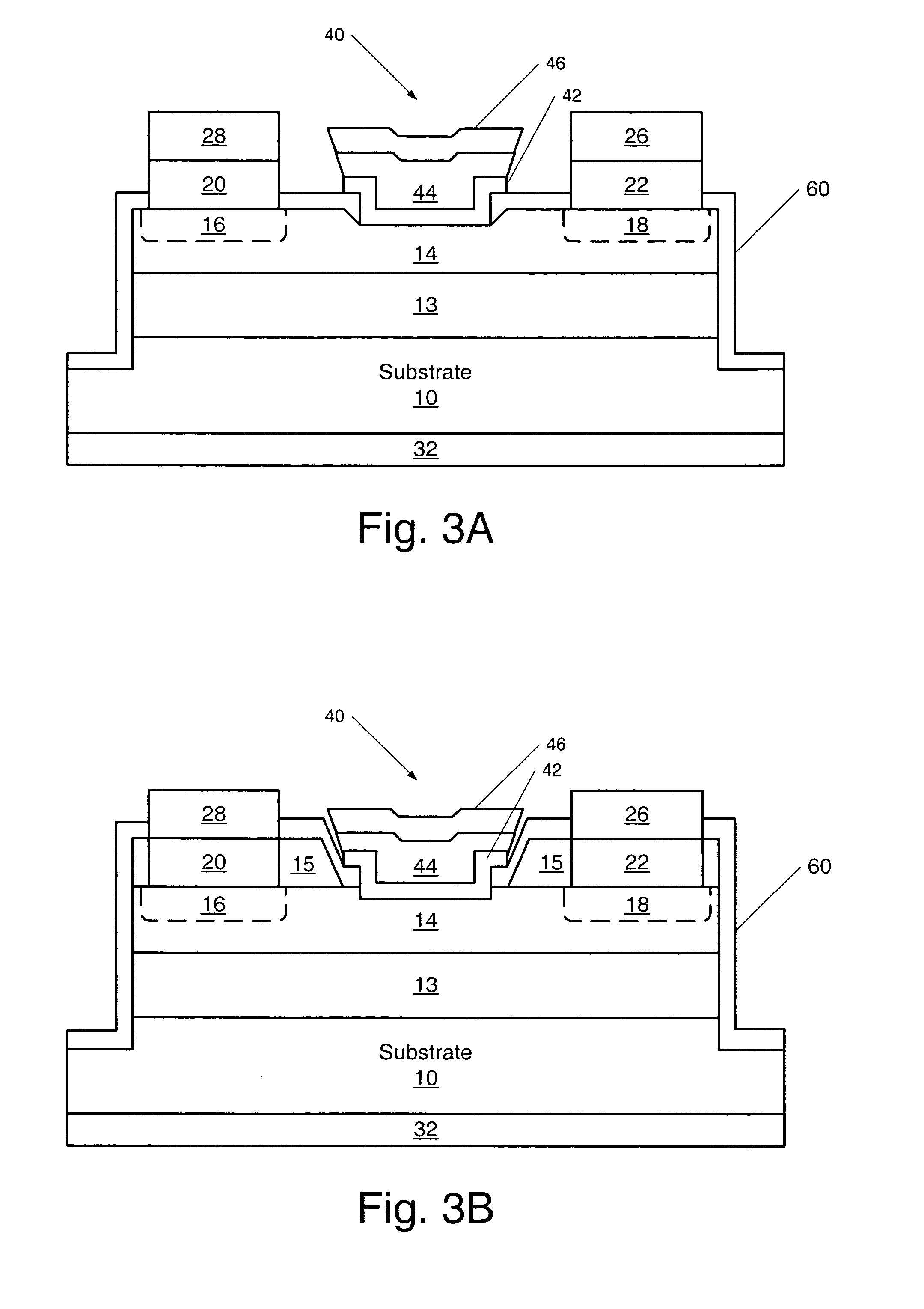
[0067]FIG. 3A illustrates a MESFET of the present invention where the Schottky gate contact 40 is recessed in the active channel layer. FIG. 3A also illustrates an embodiment of the present invention where the Schottky gate contact 40 is a mushroom gate contact. A first epitaxial layer 13 of p-type conductivity is grown on a single crystal bulk silicon carbide substrate 10 of either p-type conductivity, n-type conductivity or semi-insulating. The p-type epitaxial layer 13 may be a lightly doped p-type layer 12 as illustrated in FIG. 1 or a selectively doped p+ layer 12′ as illustrated in FIG. 2. A second epitaxial layer 14 of n-type conductivity is grown on the first epitaxial layer 13. Also illustrated in FIG. 3A are optional n+ regions 16 and 18 formed in the source and drain regions of the device which may be formed as described with reference to FIG. 2. The n+ regions 16 and 18 may be eliminated as described above with reference to FIG. 2 and illustrated in FIG. 1. Ohmic contact...


PUM


Abstract

SiC MESFETs are disclosed which utilize a semi-insulating SiC substrate which substantially free of deep-level dopants. Utilization of the semi-insulating substrate may reduce back-gating effects in the MESFETs. Also provided are SiC MESFETs with a two recess gate structure. MESFETS with a selectively doped p-type buffer layer are also provided. Utilization of such a buffer layer may reduce output conductance by a factor of 3 and produce a 3 db increase in power gain over SiC MESFETs with conventional p-type buffer layers. A ground contact may also be provided to the p-type buffer layer and the p-type buffer layer may be made of two p-type layers with the layer formed on the substrate having a higher dopant concentration. SiC MESFETs according to embodiments of the present invention may also utilize chromium as a Schottky gate material. Furthermore, an oxide-nitride-oxide (ONO) passivation layer may be utilized to reduce surface effects in SiC MESFETs. Also, source and drain ohmic contacts may be formed directly on the n-type channel layer, thus, the n+ regions need not be fabricated and the steps associated with such fabrication may be eliminated from the fabrication process. Methods of fabricating such SiC MESFETs and gate structures for SiC FETs as well as passivation layers are also disclosed.

Description

RELATED APPLICATION[0001]The present application is a divisional of and claims priority from U. S. application Ser. No. 09 / 567,717, filed May 10, 2000, now U.S. Pat. No. 6,686,616 entitled “SILICON CARBIDE METAL-SEMICONDUCTOR FIELD EFFECT TRANSISTORS,” which is assigned to the assignee of the present application, the disclosure of which is incorporated herein as if set forth fully.STATEMENT OF GOVERNMENT INTEREST[0002]The present invention was made with Government support under contract number N00014-96-C-2152 awarded by the United States Office of Naval Research. The Government has certain rights in this invention.FIELD OF THE INVENTION[0003]The present invention relates microelectronic devices and more particularly to metal-semiconductor field-effect transistors (MESFETs) formed in silicon carbide.BACKGROUND OF THE INVENTION[0004]Electrical circuits requiring high power handling capability (>20 watts) while operating at high frequencies such as radio frequencies (500 MHz), S-ba...

Claims


Application Information

Patent Timeline
Patent Type & Authority Patents(United States)
IPC IPC(8): H01L21/338H01L21/28H01L21/04H01L21/76H01L29/24H01L29/417H01L29/47H01L29/812
CPCH01L21/7605H01L29/1608H01L29/47H01L29/8128H01L29/66856H01L29/812H01L29/66068H01L29/772
Inventor ALLEN, SCOTT T.PALMOUR, JOHN W.ALCORN, TERRENCE S.
Owner CREE INC
Why Eureka
Try Eureka