Semiconductor device and method of manufacturing the same

a semiconductor and semiconductor technology, applied in the direction of semiconductor devices, electrical devices, transistors, etc., can solve the problems of uneven distribution of crystal grains with irregular grain sizes, inability to specify the position and the size of crystal grains in forming a tft, and almost impossible to remove the adverse effects of crystal grain boundary

Inactive Publication Date: 2006-07-18
SEMICON ENERGY LAB CO LTD
View PDF119 Cites 33 Cited by
  • Summary
  • Abstract
  • Description
  • Claims
  • Application Information

AI Technical Summary

Benefits of technology

[0026]The present invention has been made to solve those problems and an object of the present invention is therefore to provide a crystalline semiconductor film in which the position and the size of crystal grains are controlled, and to provide a TFT that can operate at high speed by forming a channel formation region of the TFT from the obtained crystalline semiconductor film. Another object of the present invention is to provide a technique of applying the obtained TFT to various semiconductor devices such as a transmissive liquid crystal display device and a display device that uses an electro-luminescence material.
[0027]The present invention increases the grain size of crystal grains of a crystalline semiconductor film formed by laser annealing. The invention is characterized in that the cooling process of a semiconductor film is slowed down using a heat retaining film formed between the semiconductor film and a substrate to reduce the heat loss rate of heat given by laser beam irradiation and that a reflective film is formed on a region of the semiconductor film which does not overlap the heat retaining film to create a temperature gradient in the semiconductor film, whereby crystal grains having a large grain size are formed at designed positions. The reflective film in this specification refers to a film having high reflectance. Since crystal growth length is in proportion to the product of growth time (a time period a melted semiconductor film takes to solidify) and growth rate (speed at which the solid-liquid interface moves), the grain size is increased as the cooling rate of the semiconductor film is lowered to prolong the growth time. The position of the crystal grain can also be controlled by controlling the cooling rate.
[0028]The heat retaining film is formed using a silicon oxide film that contains methyl (CH3), ethyl (C2H5), propyl (C3H7), butyl (C4H9), vinyl (C2H3), phenyl (C6H5), or CF3 group (functional group containing silicon oxide film). A silicon oxide film containing any one of the groups given above does not participate in forming a network of Si—O bonds because the functional group terminates the bonds. The heat transmission rate is thus lowered and the film works effectively as the heat retaining film. It is also effective to use a porous silicon film or a porous silicon oxide film to form the heat retaining film. Owing to the pores, heat transmission rate is low in a porous silicon film or a porous silicon oxide film to make the film useful as the heat retaining film.
[0033]The reflective film is polygonal in top view, and this polygon has an angle which is smaller than 60°. With the reflective film shaped as such, the crystal nuclei are generated at a smaller density in the semiconductor film below the vertex when the semiconductor film is irradiated with the laser beam. Thus collision between growing crystal grains can be avoided.
[0035]The substrate may be heated up to about 500° C. before the laser beam irradiation. Expectedly, this will lower the heat loss rate in the semiconductor film to increase the grain size of the crystal grains.

Problems solved by technology

However, in a crystalline semiconductor film formed by laser annealing, plural crystal grains mass, so that the crystal grains with irregular grain sizes are distributed unevenly.
With crystal grains of irregular grain sizes distributed unevenly, it is impossible to specify the position and the size of the crystal grains in forming a TFT.
While electric characteristics of a TFT heavily depend on the crystallinity of the semiconductor film for forming a channel formation region, it has been almost impossible to remove the adverse effects of crystal grain boundary and form the channel formation region from a single crystal semiconductor film.
However, such high energy region is very narrow and where a crystal grain having a large grain size is to be formed cannot be controlled.
Also, the method can control where the crystal grains are to be formed but it cannot control the formation position on a single crystal basis.
The metal film that is formed directly on the amorphous semiconductor film also can cause a problem, in that the metal elements in the film diffuse into the amorphous semiconductor film.
Furthermore, the method may cause cracking or peeling in the metal film and the amorphous semiconductor film.
Also, the buried insulating layer that is quadrangular in top view with one or more corners of the quadrangle having an angle as wide as 60° results in too many crystal nuclei in the semiconductor film below the wide corner or corners when the semiconductor film that has been melted by laser irradiation is cooled down.
These crystal grains crowd the film and collide with one another as they grow, thereby lowering possibility of obtaining crystal grains of large grain size.
Furthermore, the complicate structure of burying an insulating layer in an amorphous semiconductor film cause the trouble when it comes to forming a TFT.
The trouble is that the buried insulating layer remains despite the fact that it has nothing to do with the actual function of the TFT.
However, this top gate TFT will have difficulty in operating at high speed because the silicon oxide film provided between the amorphous semiconductor film and the high melting point metal film generates parasitic capacitance to increase current consumption.
Thus the method cannot satisfy the optimal design for crystallization process and the optimal design for element structure simultaneously.
Moreover, when a high melting point metal film that does not transmit light is formed over the entire-surface of a glass substrate, it cannot form a transmissive liquid crystal display device.
Also, a chromium (Cr) film or a titanium (Ti) film used as the high melting point metal film has high internal stress, which probably leads to insufficient adhesion to the glass substrate.
The high internal stress also influences the semiconductor film to be formed above the high melting point metal film and is likely to cause distortion in the resultant crystalline semiconductor film.
Therefore, there is a fear that the high melting point metal film provided between the substrate and the base film will disturb the balance.
The SLS method requires control with a micron-level precision in positioning the mask relative to the substrate, thereby making the laser irradiation apparatus for this method more complicated than an ordinary one.
Moreover, the method has a problem in throughput when it is used to form a TFT for a liquid crystal display device having a large area region.

Method used


Image

  • Semiconductor device and method of manufacturing the same
  • Semiconductor device and method of manufacturing the same
  • Semiconductor device and method of manufacturing the same

Examples


embodiment 1

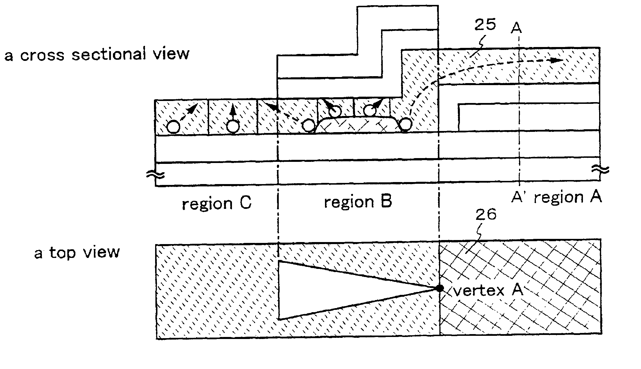
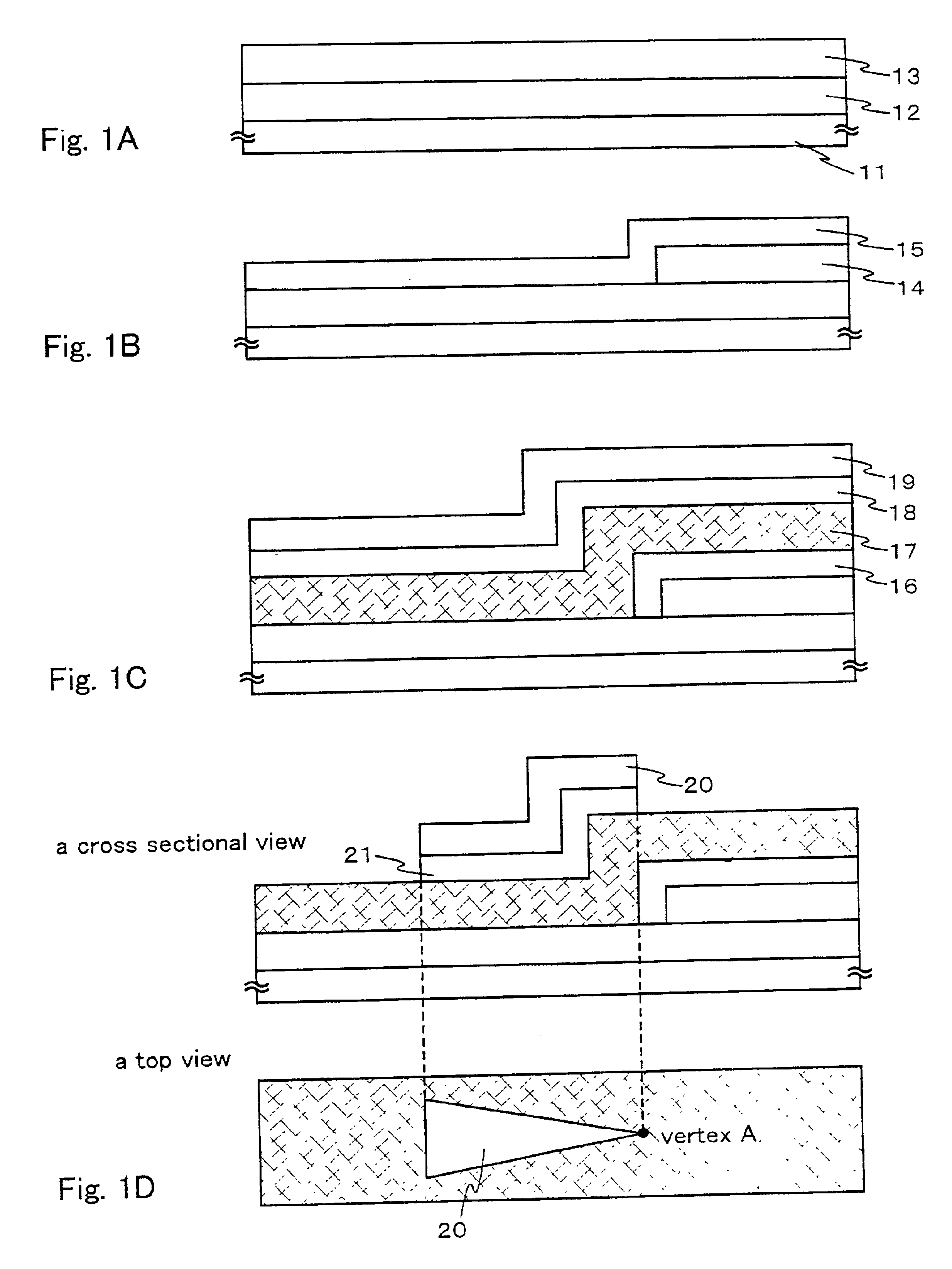
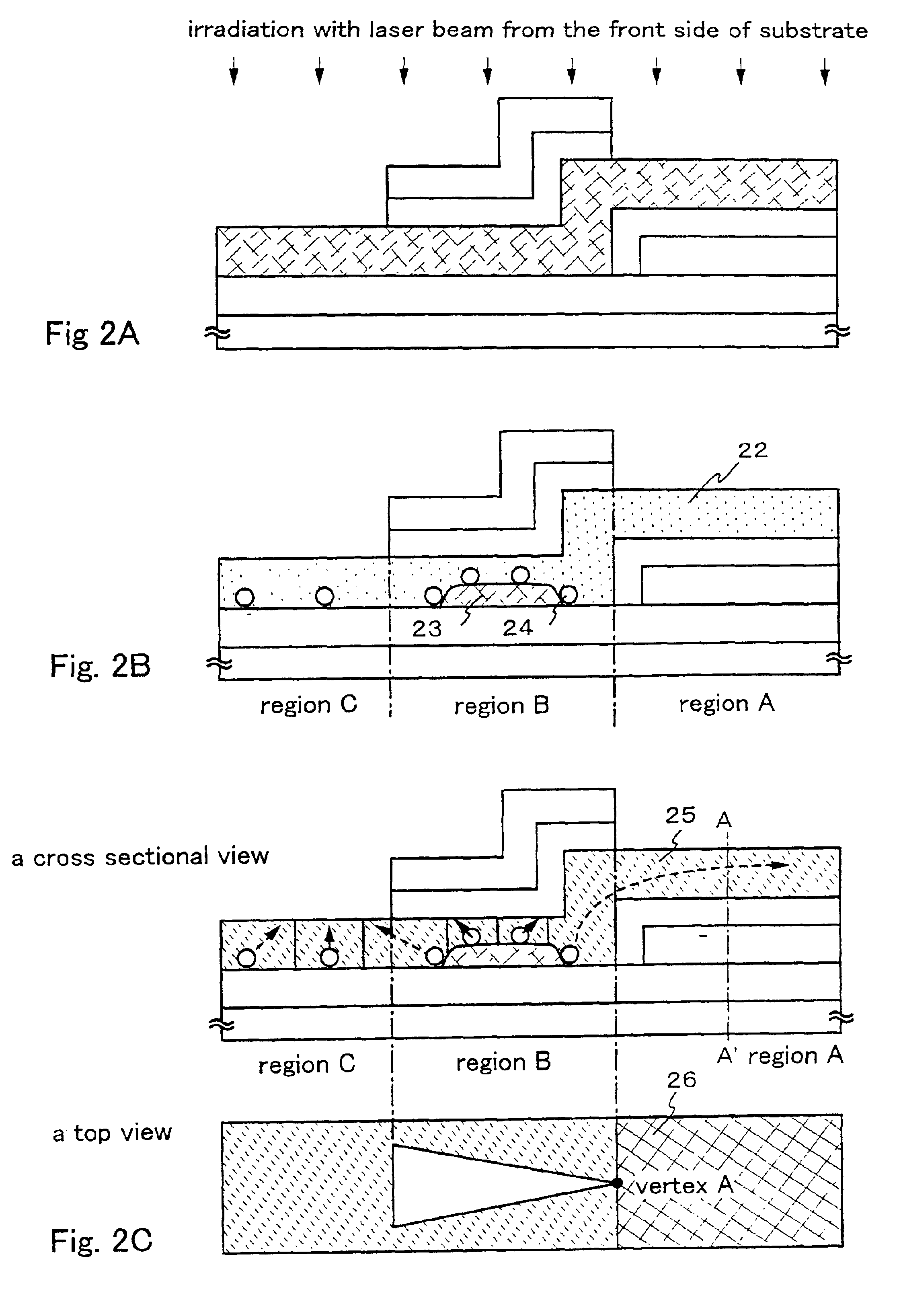
[0074]Embodiment 1 of the present invention will be described with reference to cross sectional views of FIGS. 1A to 2C. In FIGS. 1D and 2C, top views as well as cross sectional views are shown.

[0075]In FIG. 1A, a substrate is denoted by 11. The substrate 11 may be a glass substrate. Examples of the glass substrate include a synthesized quartz glass substrate, and a non-alkaline glass substrate such as a barium borosilicate substrate or an aluminoborosilicate glass substrate. Transparent films such as PC (polycarbonate), PAr (polyarylate), PES (polyether sulfon) and PET (polyethylene telephthalate) may be used instead. For example, Corning No. 7059 glass or No. 1737 glass (product of Corning Incorporated.) is a preferable material for the substrate 11.

[0076]A base insulating film 12 is formed on the substrate 11 by a known method (LPCVD, plasma CVD, or the like) from a silicon nitride film, a silicon oxynitride film, a silicon oxide film or a like other film. In this embodiment, a s...

embodiment 2

[0092]This embodiment shows an example of forming a crystalline semiconductor film by a method different from the one described in Embodiment 1. The only difference between this embodiment and Embodiment 1 is in the step of forming the heat retaining film 13 and the subsequent steps are identical. Therefore explanations for the identical steps are omitted here.

[0093]First, a substrate is prepared as in Embodiment 1. The substrate, denoted by 11, may be a glass substrate. Examples of the glass substrate include a synthesized quartz glass substrate, and a non-alkaline glass substrate such as a barium borosilicate substrate or an aluminoborosilicate glass substrate. Transparent films such as PC (polycarbonate), PAr (polyarylate), PES (polyether sulfon) and PET (polyethylene telephthalate) may be used instead. For example, Corning No. 7059 glass or No. 1737 glass (product of Corning Incorporated) is a preferable material for the substrate 11.

[0094]A base insulating film 12 is formed on ...

embodiment 3

[0099]This embodiment shows an example of forming a crystalline semiconductor film by a method different from the ones described in Embodiments 1 and 2. The only difference between this embodiment and Embodiment 1 is in the step of forming the heat retaining film 13 and the subsequent steps are identical. Therefore explanations for the identical steps are omitted here.

[0100]First, a substrate is prepared as in Embodiment 1. The substrate, denoted by 11, may be a glass substrate. Examples of the glass substrate include a synthesized quartz glass substrate, and a non-alkaline glass substrate such as a barium borosilicate substrate or an aluminoborosilicate glass substrate. Transparent films such as PC (polycarbonate), PAr (polyarylate), PES (polyether sulfon) and PET (polyethylene telephthalate) may be used instead. For example, Corning No. 7059 glass or No. 1737 glass (product of Corning Incorporated) is a preferable material for the substrate 11.

[0101]A base insulating film 12 is fo...


PUM


Abstract

A crystalline semiconductor film in which the position and the size of crystal grains are controlled is provided, and a TFT that can operate at high speed is obtained by forming a channel formation region of the TFT from the crystalline semiconductor film. A heat retaining film is formed on an insulating surface, a semiconductor film is formed to cover the heat retaining film, and a reflective film is formed to partially cover the semiconductor film. The reflective films and the semiconductor film are irradiated with a laser beam. The reflective film creates a distribution in effective irradiation intensity of laser beam on the semiconductor film. The distribution, with the heat retaining effect provided by the heat retaining film, generates a temperature gradient in the semiconductor film. Utilizing these, the position where crystal nuclei are to be generated and the direction in which crystal growth should advance can be controlled and crystal grains having a large grain size can be obtained.

Description

BACKGROUND OF THE INVENTION[0001]1. Field of the Invention[0002]The present invention relates to a method of manufacturing a semiconductor device having circuits that are composed of thin film transistors (hereinafter referred to as TFTs). Specifically, the invention relates to the structure of electro-optical devices represented by liquid crystal display devices and of electric appliances having as their parts the electro-optical devices, and the invention also relates to how to manufacture the devices. The term semiconductor device herein refers to a device in general which utilizes semiconductor characteristics to function, and the electro-optical devices and electric appliances described above fall within this category.[0003]2. Description of the Related Art[0004]A technique that has been a popular research subject in recent years is to use laser annealing to crystallize an amorphous semiconductor film formed on an insulating substrate such as a glass substrate or to improve cry...

Claims


Application Information

Patent Timeline
Patent Type & Authority Patents(United States)
IPC IPC(8): H01L21/20H01L21/336H01L21/77H01L29/04H01L29/786
CPCH01L27/1281H01L27/1296H01L29/04H01L29/78621H01L29/78675H01L29/66757H01L2029/7863
Inventor YOSHIMOTO, SATOSHI
Owner SEMICON ENERGY LAB CO LTD
Why Eureka
Try Eureka