In the manufacturing of semiconductor devices, as the dimensions have shrunk, it has become more challenging to provide dielectric film
layers that provide adequate
electrical isolation between interconnect features and device components in order to minimize RC
delay and
crosstalk.
However, the CVD processes, in particular PECVD, may not adequately fill the spaces or gaps between existing
metal features, and may leave voids in the dielectric
blanket layer which can cause problems such as micro-
cracking, lack of structural support,
trapping of gases or
moisture or allow subsequent
metal fill processes to connect nearby voids which can result in shorted device elements.
Although films provided by spin-on deposition may adequately fill spaces or gaps, these films are usually porous and would be incompatible with other MOL
processing steps by being susceptible to problems such as those mentioned above.
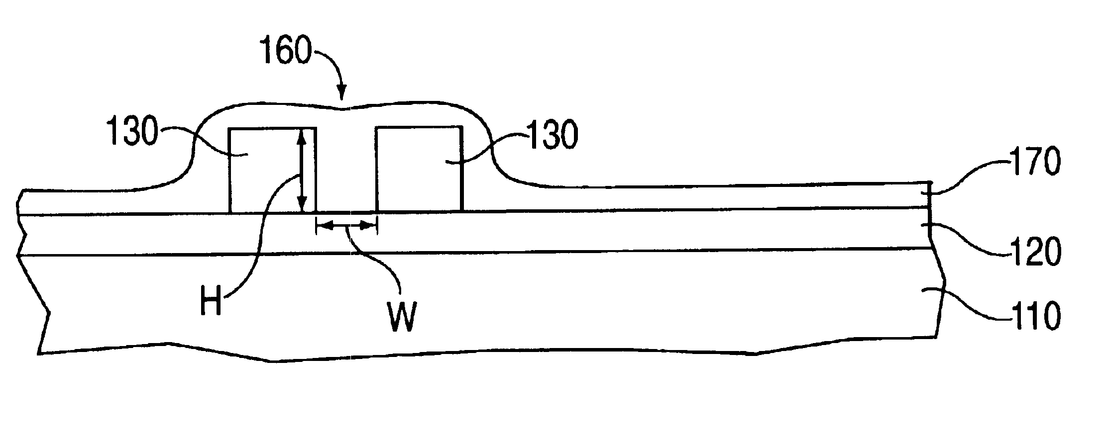
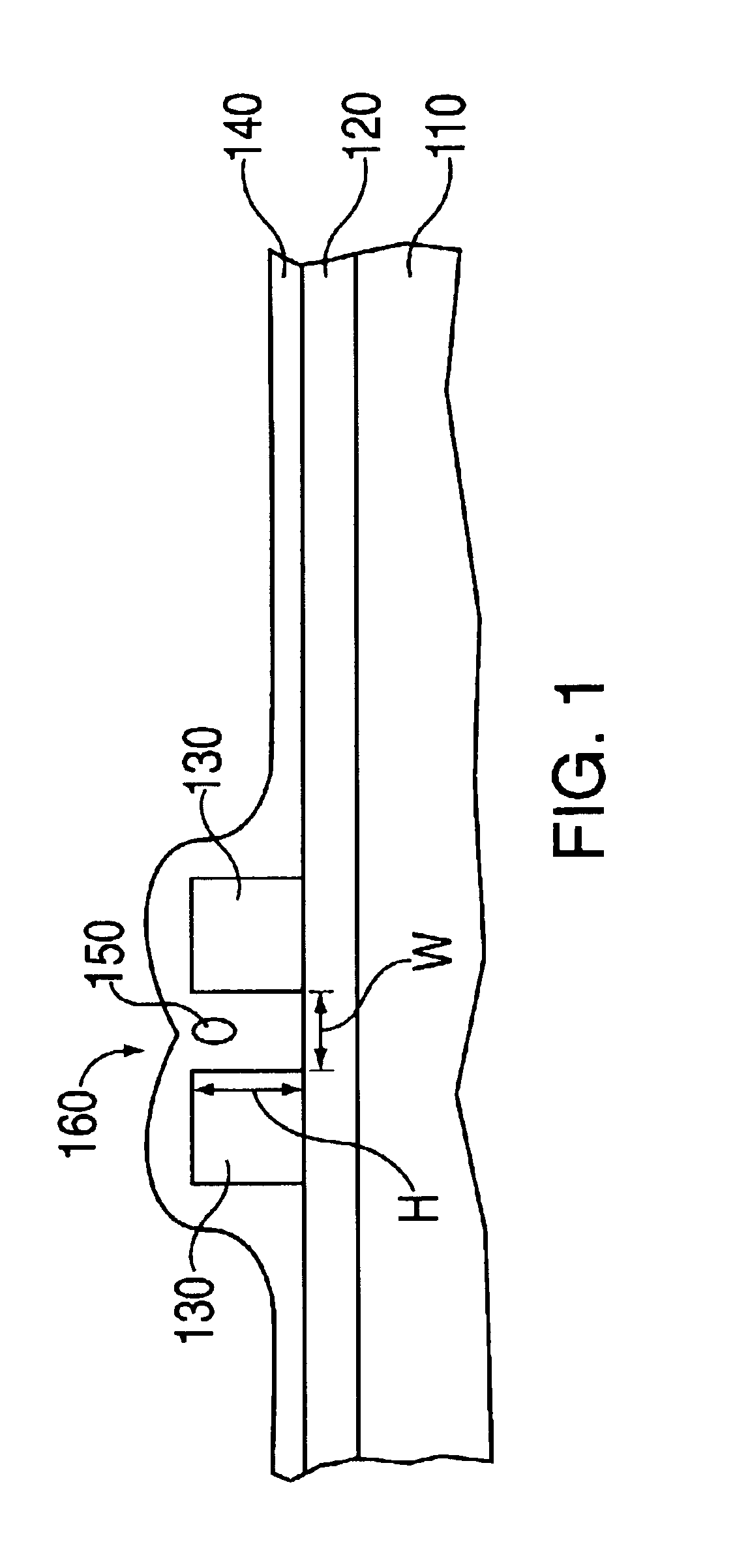
The problem of adequate gap fill can be particularly difficult if the
aspect ratio (AR), which is the ratio of height to width of the gaps, is above about 1.0.
However, PECVD solutions at the MOL level are not easily utilized, because PECVD processes may leave voids in high
aspect ratio gaps, where the gap AR exceeds about 1.0.
In addition,
plasma processing is not a preferred fill method for MOL as it may cause charge damage to gate oxides.
However, using low-k materials for AR greater than 1, SACVD may also leave voids depending on the shape of the gap to be filled.
However, because the
process conditions for depositing low-k films that would also provide good gap-filling results are quite sensitive to the composition of reactant gases and the structure of the gaps to be filled, the addition of dopants which reduce the reflow temperature would not necessarily preserve the desired low-k and gap-filling properties of the film, and may require significant experimentation to achieve the desired results.
However, the increased concentration of hydroxyl radicals may lead to a
porous film that is incompatible with MOL processing and increased concentration of hydroxyl radicals will result in reduced carbon incorporation in the film.
Since carbon incorporation is required to achieve a low-k
oxide, the Sukarev patent does not provide a solution for depositing low-k dielectric films that provide good
gap filling results.
Moreover, the use of UV
radiation to increase deposition rates may require modification of standard reaction chambers and may increase the cost of processing.
In addition, the preferred embodiment of the Yuan patent requires movement of the
wafer through the reactor, which adds to the complexity of the
reactor design.
Movement of the
wafer also results in variation in
elemental composition with depth across the substrate and therefore the etch rate will vary with depth, which is incompatible with MOL processing steps such as wet HF etch.
In addition, the Yuan patent is not directed to the deposition of low-k dielectric films, which would require strict compositional and density control that is beyond the capability of the Yuan patent.
The Saito patent also requires the movement of the wafer relative to the gas
injector, adding complexity to the
reactor design and suffers from similar compositional deficiencies as in the Yuan patent.
Therefore, the Saito patent is not suitable for the deposition of low-k dielectrics that provide good gap-filling for AR greater than about 3.
Thus, the method of the Rose patent does not recognize the
disadvantage of potential charge damage due to the use of
plasma CVD processes.
The Rose patent also does not solve the problem of gap-fill for AR greater than 1.
Since the Ravi patent teaches the use of a PECVD process and does not suggest the use of a carbon-containing cyclosiloxane precursor such as TMCTS or OMCTS, the Ravi patent is not suitable for depositing low-k dielectric films which have good gap fill characteristics for AR greater than about 1.
Also, the method of the Ravi patent suffers from potential charge damage due to
plasma processing.
In addition, the method of the Laboda reference does not provide good gap-filling characteristics for AR greater than about 1.

