Optoelectronic probe

a technology of optoelectronic probes and probes, applied in the direction of liquid/fluent solid measurement, peptides, test/measurement of semiconductor/solid device, etc., can solve the problems of difficult extreme complexity, and achieve the reduction of voltage drop on the oxide layer, the effect of reducing the dark current and the difficulty of analysis of impedance spectroscopy

Inactive Publication Date: 2006-08-08
LIN HAIAN
View PDF13 Cites 7 Cited by
  • Summary
  • Abstract
  • Description
  • Claims
  • Application Information

AI Technical Summary

Benefits of technology

[0026]The first advantage for the present invention is that the size of the electrode is self-defined by the size of light beam. It will be easy to adjust the electrode size to match a single cell by simply adjusting beam size. Therefore we are able to characterize a single cell in a convenient way. On the other hand, a large beam size can also be used to assemble a particle array. This is very different from the Optical Tweezer where the trapping zone is too small (on the order of the light wavelength) to manipulate the particle array.
[0027]The second advantage for the present invention is that an inversion region is used as a working electrode. The inversion layer has behavior similar to a metal electrode. The most of applied electric field can be shielded by the inversion layer and no significant field will penetrate into the semiconductor bulk. In addition, a majority carrier tunneling process will also reduce voltage drop on the oxide layer. Therefore a significant portion of bias will be dropped into the electrolyte. Furthermore, the metal-like electrode formed by the inversion layer is also perfect for the impedance characterization. This is very different from the conventional illumination-assisted field induced assembly technologies (or a conventional optoelectronic tweezers), where the semiconductor bulk or depletion region plays as the electrode. The involvement of the depletion region at the semiconductor surface will cause an extreme complexity on the voltage distribution among the different part of the “sandwich” electrochemical cell and make it very diff

Problems solved by technology

The involvement of the depletion region at the semiconductor surface will cause an extreme complexity on the voltage distribution

Method used


Image

  • Optoelectronic probe
  • Optoelectronic probe
  • Optoelectronic probe

Examples


Embodiment Construction

[0040]The following description is of the best mode presently contemplated for the carrying out of the invention. This description is made for the purpose of illustrating the general principles of the invention, and is not to be taken in a limiting sense. The scope of the invention is best determined by reference to the appended claims.

I. Optoelectronic Probe

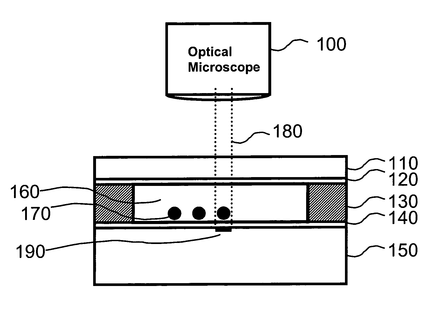
[0041]FIG. 1 is a sectional view of an embodiment of the present invention. An optical microscope, represented by reference number 100, can be used to observe and record the particle manipulation process. The top electrode of the “sandwich” electrochemical cell is formed by a glass slide 110 coated by an optically transparent conducting thin film, such as indium tin oxide (ITO) 120. This kind of transparent conducting electrode is commercially available. A spacer (typically thick ˜50 μm), represented by reference number 130, is formed by polymer film with a hole in the center. Reference numeral 140 denotes a layer of thin oxide ...


PUM

PropertyMeasurementUnit
Timeaaaaaaaaaa
Thicknessaaaaaaaaaa
Polarityaaaaaaaaaa

Abstract

The present invention, referred to as optoelectronic probe, concerns a novel apparatus and method for characterization and micromanipulation of particles or biomolecules in an electrolyte solution. Electric fields, which include both time constant and time-varying components, are applied to a thin insulating layer covered, lightly doped semiconductor material. Illumination injects carriers into the insulator/semiconductor interface to compensate the leaking minority carrier current and maintain an inversion layer, which works as an electrode to control the particle movements. A particle array, or even a single cell, can be assembled in, or moved along with the inversion layer electrode, which is induced by illumination. Furthermore, an impedance analyzer is utilized to characterize the trapped particles, or single cell. The present invention has numerous uses, such as bio-chemical analysis systems, and nanosize structures assembly for electronic or optical devices.

Description

CROSS-REFERENCE TO RELATED APPLICATIONS[0001]Not ApplicableSTATEMENT REGARDING FEDERALLY SPONSORED RESEARCH OR DEVELOPMENT[0002]Not ApplicableREFERENCE TO SEQUENCE LISTING, A TABLE, OR A COMPUTER PROGRAM LISTING COMPACT DISK APPENDIX[0003]Not ApplicableBACKGROUND OF THE INVENTION[0004]1. Field of Invention[0005]The present invention is directed generally to methods and apparatus based on optoelectronic effect, electro / dielectro-phoresis, and impedance spectroscopy, in order to trap, move, deform and characterize particles, such as cells, molecules, any type of colloids, any of inorganic and bio-organic substances, beads, as well as pucks and like small things. “Optoelectronic Probe” refers to the invention described herein.[0006]2. Background of the InventionI. Optical Tweezers[0007]The manipulation of micro- or nano-size particles is considered as the key for the new generation of photonic, optoelectronic, and electronic devices, as well as biochemical analysis systems. Optical twe...

Claims


Application Information

Patent Timeline
IPC IPC(8): G01R27/08G01R31/26H01L21/66
CPCG01R1/071
Inventor LIN, HAIAN
Owner LIN HAIAN
Why Eureka
Try Eureka