Manufacturing method of semiconductor device

a manufacturing method and semiconductor technology, applied in semiconductor devices, electrical equipment, instruments, etc., can solve the problems of voltage drop, the influence of voltage drop cannot be neglected after, and the uniformity of an image quality is significantly damaged in a pixel portion, so as to reduce wiring resistance, reduce voltage drop, and make large current flow

Inactive Publication Date: 2006-08-22
SEMICON ENERGY LAB CO LTD
View PDF54 Cites 57 Cited by
  • Summary
  • Abstract
  • Description
  • Claims
  • Application Information

AI Technical Summary

Benefits of technology

[0024]In the present invention, the wiring including copper is formed to enable making large current flow as well as reducing wiring resistance. Accordingly, it is possible to reduce voltage drop and a round of a signal waveform.
[0025]In addition, in the present invention, an area occupied by wirings and electrodes can be reduced since microfabrication of the wiring including copper is possible. It is noted that it is especially effective in the case of manufacturing a middle-sized or large-sized panel with a size of 5 inch or more and making large current flow into a wiring to use the wiring including copper in accordance with the present invention.

Problems solved by technology

There is, however, voltage drop (also referred to as IR drop) due to a wiring resistance as a phenomenon that becomes a problem in driving a display device, which is a phenomenon that a voltage is more lowered as a distance from a power source is larger in the same wiring.
This problem is especially serious in the case of a long wiring length, and is a barrier against the achievement of a large screen of the display device.
Namely, the voltage drop due to the wiring resistance makes it impossible to transmit a desired voltage, which causes as the result a trouble that uniformity of an image quality is significantly damaged in a pixel portion.
However, the influence of the voltage drop cannot be neglected after all since the wiring is taken around long.
In the case of fabricating a monolithic display device in which a driving circuit portion (typically including a gate driving circuit and a source driving circuit) is formed integrally on the same substrate, a wiring resistance of a wiring taken around between the driving circuit portion and an input terminal for an electric signal becomes a problem.
The wiring resistance is likely to cause delay in the electric signal to lower an operation speed of the gate driving circuit or the source driving circuit.
As set forth above, there are troubles that uniformity of an image quality is significantly damaged and an operation speed of the driving circuit portion is extremely lowered by the voltage drop due to the wiring resistance and the delay in the electric signal.
Such problem is especially serious in the case of a display device that has a large-sized screen with diagonally several tens inch.
In such case, however, microfabrication is difficult and particle contamination is caused in using CMP since copper is used as the material with low resistance and a copper wiring is formed with damascene.

Method used


Image

  • Manufacturing method of semiconductor device
  • Manufacturing method of semiconductor device
  • Manufacturing method of semiconductor device

Examples


embodiment mode 1

[Embodiment Mode 1]

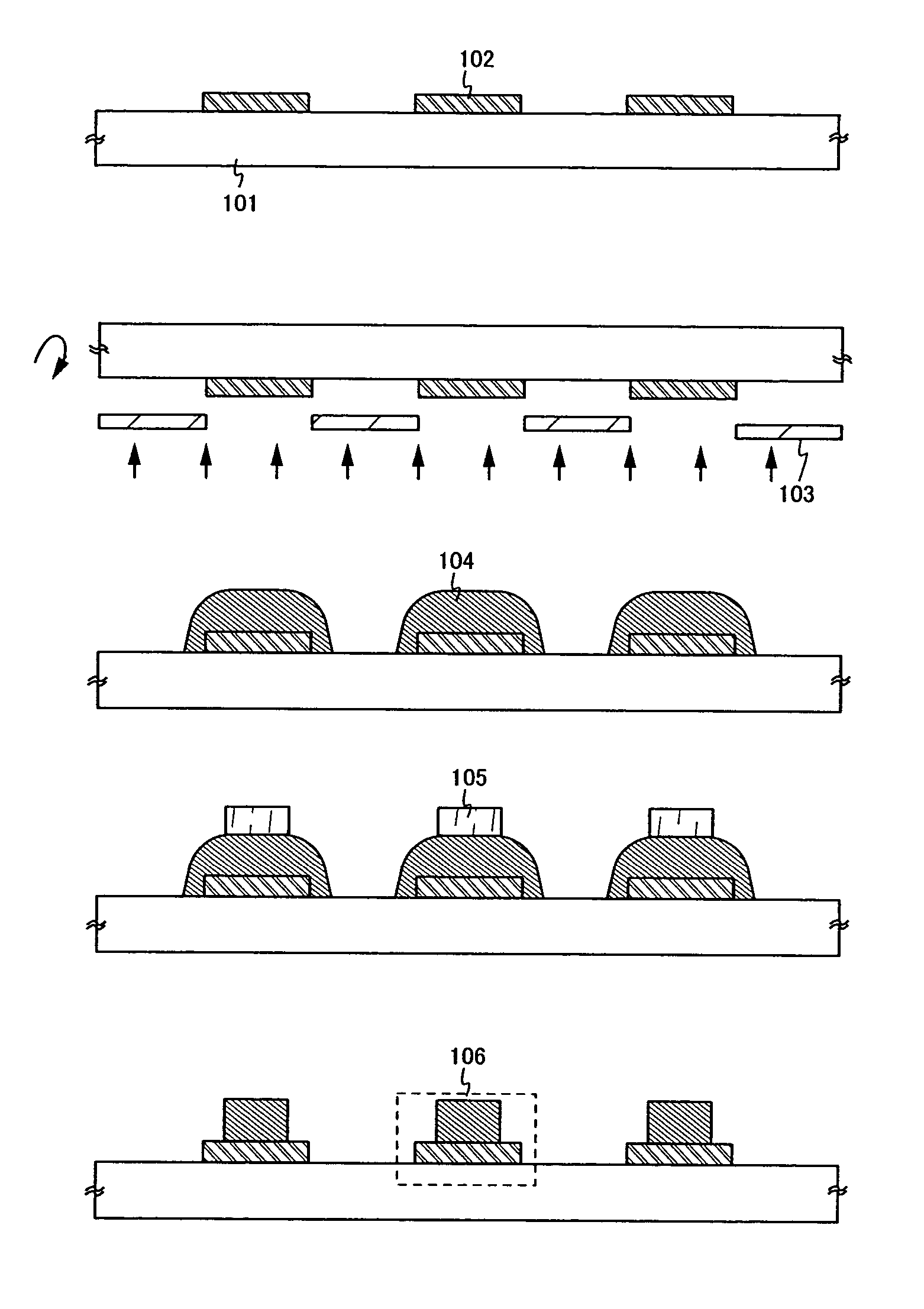
[0037]A manufacturing method of a wiring including copper according to the present invention will be described with FIGS. 1A to 1E.

[0038]In FIG. 1A, pattern formation is performed to form a first conductive film 102 on a substrate 101. As the first conductive film 102 formed here, it is possible to use a film such as a conductive film including TiN (titanium nitride), TaN (tantalum nitride), WN (tungsten nitride), TiC (titanium carbide), TaC (tantalum carbide), or Si (silicon) that has a property as a barrier for preventing penetration of copper from a later formed conductive film including copper. In addition, materials such as Ti, Al, Ta, and W can be used in combination with the materials mentioned above.

[0039]The first conductive film is formed with sputtering and subjected to patterning with dry etching to have a line width of 30 to 40 μm.

[0040]Next, pattern formation is performed using sputtering with a mask 103 as shown in FIG. 1B to form a second conductiv...

embodiment mode 2

[Embodiment Mode 2]

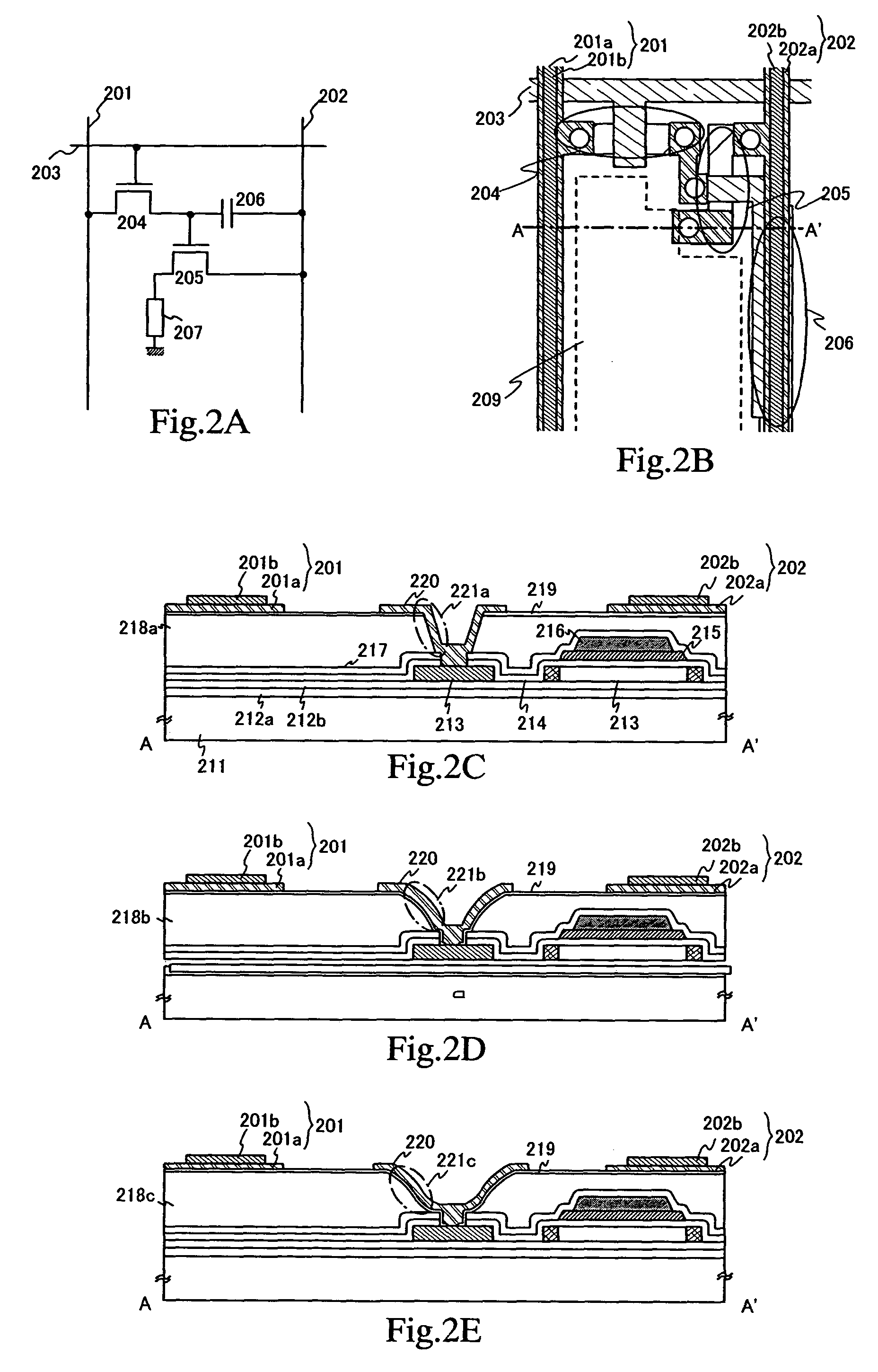
[0044]In the present embodiment mode, an explanation will be given on the case that a wiring including copper is used for a signal line (a current supply line is also included in the present embodiment mode) formed in a pixel portion of a display device for inputting a signal from a source driving circuit to each pixel. It is noted that a light emitting device that has a light emitting element with an electroluminescent layer formed to be sandwiched between a pair of electrodes is used as the display device shown in the present embodiment mode.

[0045]The light emitting device has plural pixels shown in FIG. 2A in a matrix shape in a pixel portion, and each pixel has a signal line 201, a current supply line 202, a scan line 203, plural TFTs 204 and 205, a capacitor 206, and a light emitting element 207. It is noted that the TFTs 204 and 205 may have a multi-gate structure such as a double-gate structure or a triple-gate structure instead of a single-gate structure.

[...

embodiment mode 3

[Embodiment Mode 3]

[0083]In the present embodiment mode, an example in which a wiring including copper is applied to a gate electrode will be described with reference to FIGS. 6A to 6C.

[0084]FIG. 6A shows an equivalent circuit of a pixel in a light emitting device. As shown in FIG. 6A, the pixel has at least a signal line 601, a current supply line 602, a scan line 603, plural TFTs 604 and 605, a capacitor 606, and a light emitting element 607. It is noted that the TFTs 604 and 605 may have a multi-gate structure such as a double-gate structure or a triple-gate structure instead of a single-gate structure.

[0085]Further, FIG. 6B shows a top view of FIG. 6A in which a pixel electrode (a first electrode of the light emitting element) 622 is formed, and has the signal line 601, the current supply line 602, the scan line 603, TFTs 604 and 605, the capacitor 606, and the pixel electrode 622 of the light emitting element. As the scan line 603 and a gate electrode of the TFT 604, a barrier ...


PUM

PropertyMeasurementUnit
thicknessaaaaaaaaaa
sizeaaaaaaaaaa
widthaaaaaaaaaa

Abstract

It is an object of the present invention to suppress an influence of voltage drop due to wiring resistance to make an image quality of a display device uniform. In addition, it is also an object of the present invention to suppress delay due to a wiring for electrically connecting a driving circuit portion to an input/output terminal to improve an operation speed in the driving circuit portion.
In the present invention, a wiring including copper for realizing lowered wiring resistance, subjected to microfabrication, is used as a wiring used for a semiconductor device and a barrier conductive film for preventing diffusion of copper is provided for a TFT as a part of the wiring including copper to form the wiring including copper without diffusion of copper into a semiconductor layer of the TFT. The wiring including copper is a wiring including a laminate film of at least a conductive film containing copper as its main component, subjected to microfabricaiton, and the barrier conductive film.

Description

BACKGROUND OF THE INVENTION[0001]1. Field of the Invention[0002]The present invention relates to wiring formation in the field of a semiconductor device that has a semiconductor element (typically, a transistor) used as a device, and belongs to technical fields on lowering resistance of a wiring and miniaturization thereof.[0003]2. Description of the Related Art[0004]There have recently been developed techniques of manufacturing a TFT with using a thin semiconductor film (a thickness on the order of several hundreds to several thousands nm) formed on an insulating surface. The TFT is widely applied to an integrated circuit (IC) and a semiconductor device such as an electro-optical device, and has been rapidly developed particularly as a switching element of display devices including a liquid crystal display device and a light emitting device.[0005]Above all, the application of display devices such as a monitor and a television has been expanded and mass production of the display dev...

Claims


Application Information

Patent Timeline
Patent Type & Authority Patents(United States)
IPC IPC(8): H01L21/4763H01L21/00H01L21/84G02F1/1362H01L21/768
CPCG02F1/136286H01L21/76841H01L21/76838G02F2001/136295H01L2221/1078G02F1/136295
Inventor YAMAZAKI, SHUNPEIOSAME, MITSUAKI
Owner SEMICON ENERGY LAB CO LTD
Why Eureka
Try Eureka