Laser annealer and laser thin-film forming apparatus

a technology of laser annealer and thin film forming apparatus, which is applied in the direction of vacuum evaporation coating, manufacturing tools, coatings, etc., can solve the problems of inability to use crystal growth techniques utilizing temperatures higher than 600° c. for the formation of polysilicon films, unstable optical output power of xecl excimer laser, and polysilicon film siz

Inactive Publication Date: 2006-09-26
FUJIFILM HLDG CORP +1
View PDF12 Cites 25 Cited by
  • Summary
  • Abstract
  • Description
  • Claims
  • Application Information

AI Technical Summary

Benefits of technology

[0044]Therefore, unlike in the conventional case, it is not necessary to move the solid material in its width direction or scan the solid material with a laser beam to illuminate the entire surface of the solid material with the laser beam.

Problems solved by technology

The deformation temperature of glass is as low as 600° C., and crystal growth techniques utilizing temperatures higher than 600° C. cannot be used for formation of a polysilicon film.
The optical output power of the XeCl excimer laser is unstable and the output light intensity varies in a range of ±10%.
When it is applied to ELA, the crystal grain size of a polysilicon film varies and the reproducibility is low.
Thus, forming continuous crystal grain boundaries is difficult and high carrier mobility cannot be obtained.
Also annealing cannot be performed at high speed in a large area.
Further, the XeCl excimer laser has problems unique to gas lasers.
The use of the XeCl excimer laser causes that the profile of a line-shaped beam is not uniform because the optical output power of the XeCl excimer laser is unstable and the output light intensity varies in a range of ±10%.
With this example, amorphous silicon does not absorb light sufficiently and the heat generation efficiency is low at a low-power oscillation wavelength 532 nm.
The annealing rate is serious in realizing mass-production and enabling processing of a large-side substrate.
Hence the film formation rate is low and the production efficiency is low.
Furthermore, the ArF excimer laser 140 is expensive and its life is as short as about 5×10⁷ shots.
Its running cost is high.
Thus, this apparatus cannot be used for thin-film formation for a product having a large film formation area such as Si-TFTs for a liquid crystal display, a solar cell, or the like.

Method used


Image

  • Laser annealer and laser thin-film forming apparatus
  • Laser annealer and laser thin-film forming apparatus
  • Laser annealer and laser thin-film forming apparatus

Examples


first embodiment

Configuration of Laser Annealer

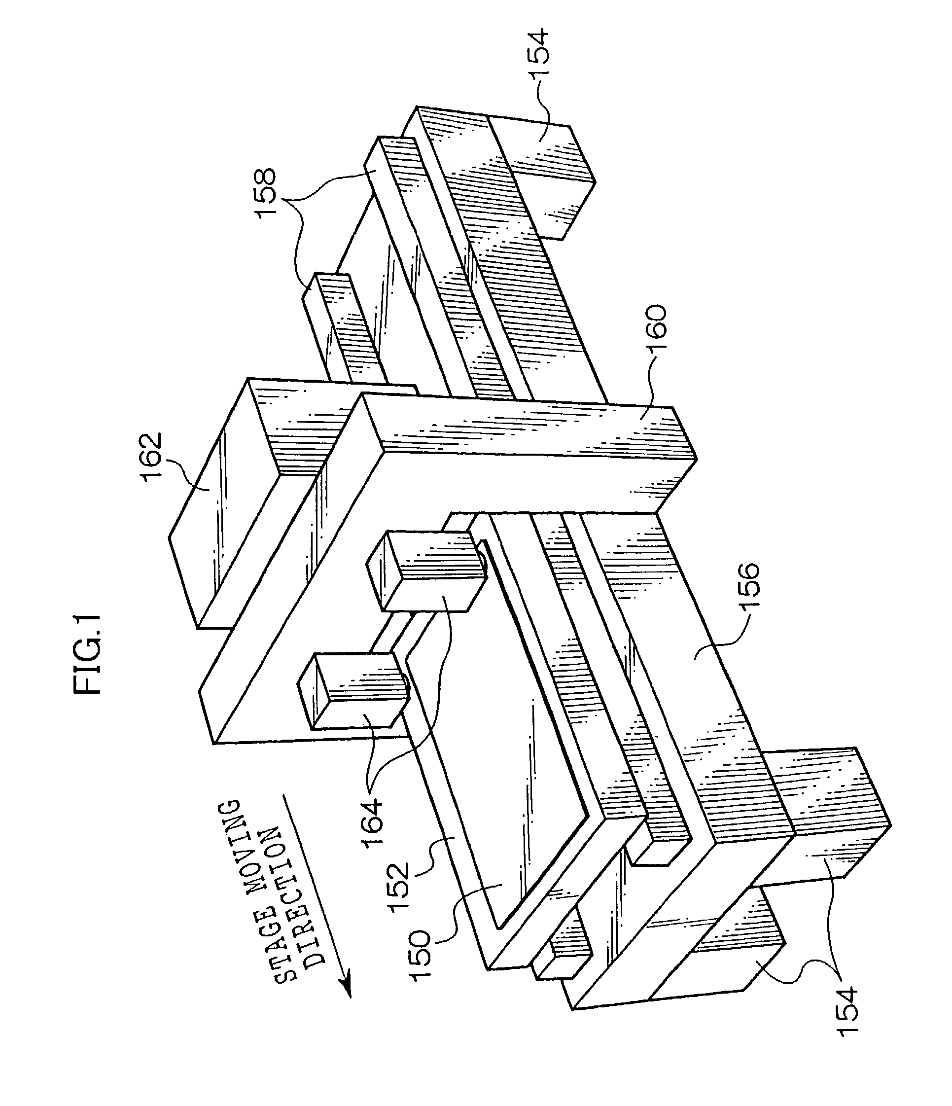
[0105]As shown in FIG. 1, a laser annealer according to the first embodiment of the invention is equipped with a flat-plate stage 152 for holding a transparent substrate 150 on which an amorphous silicon film is deposited by absorbing the substrate 150 on its surface. Two guides 158 extending along the stage moving direction are provided on a thick-plate support stage 156 that is supported by four legs 154. The stage 152 is disposed such that its longitudinal direction is parallel with the stage moving direction, and is supported by the guides 158 so as to be able to reciprocate. The laser annealer is equipped with an unillustrated driving device for driving the stage 152 along the guides 158.

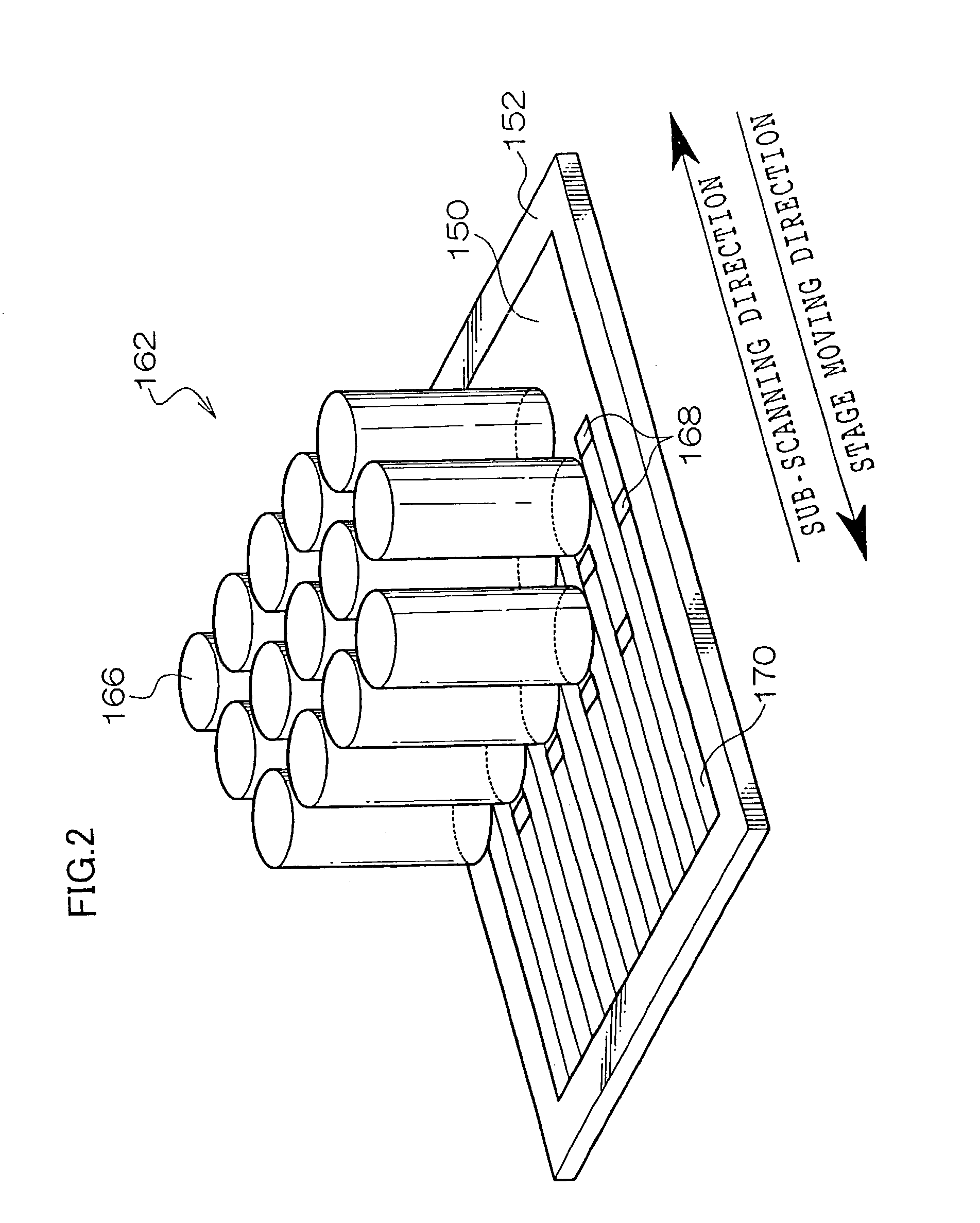
[0106]A bracket-shaped gate 160 is disposed at the center of the support stage 156 so as to stride the movement path of the stage 152. Respective end of the bracket-shaped gate 160 is fixed to both sides of the support stage 156. A scanner 162 is disposed on one s...

second embodiment

[0178]A laser annealer according to the second embodiment is such that a grating light valve (GLV) is used as a spatial light modulator in each of the illumination heads 16611 to 166mn. As disclosed in U.S. Pat. No. 5,311,360, for example, the GLV is a kind of MEMS (microelectromechanical systems)-type spatial light modulator and is a reflection diffraction grating type spatial light modulator. In the other points, the laser annealer according to the second embodiment is approximately the same as that according to the first embodiment that has been described above with reference to FIGS. 1–14. Thus, components common to the first embodiment will not be described.

[0179]In this embodiment, as shown in FIGS. 31, 32A, and 32B, each of the illumination heads 16611, to 166mn is equipped, as a spatial light modulator for modulating an incident light beam on a pixel-by-pixel basis in accordance with image data, with a GLV 300 that is long in a prescribed direction (i.e., line-shaped). As in...

third embodiment

[0197]As shown in FIGS. 35, 36A, and 36B, a laser annealer according to a third embodiment is configured in approximately the same manner as the laser annealer according to the first embodiment shown in FIG. 1 except that the scanner 162 is equipped with only a single illumination head 500 and that the illumination head 500 does not have a spatial light modulator. The same components as in the first embodiment will not be described.

[0198]In this embodiment, as shown in FIG. 35, the scanner 162 is equipped with only the single illumination head 500 for annealing. An illumination area 502 of the illumination head 500 has a long line shape extending perpendicularly to the auxiliary scanning direction.

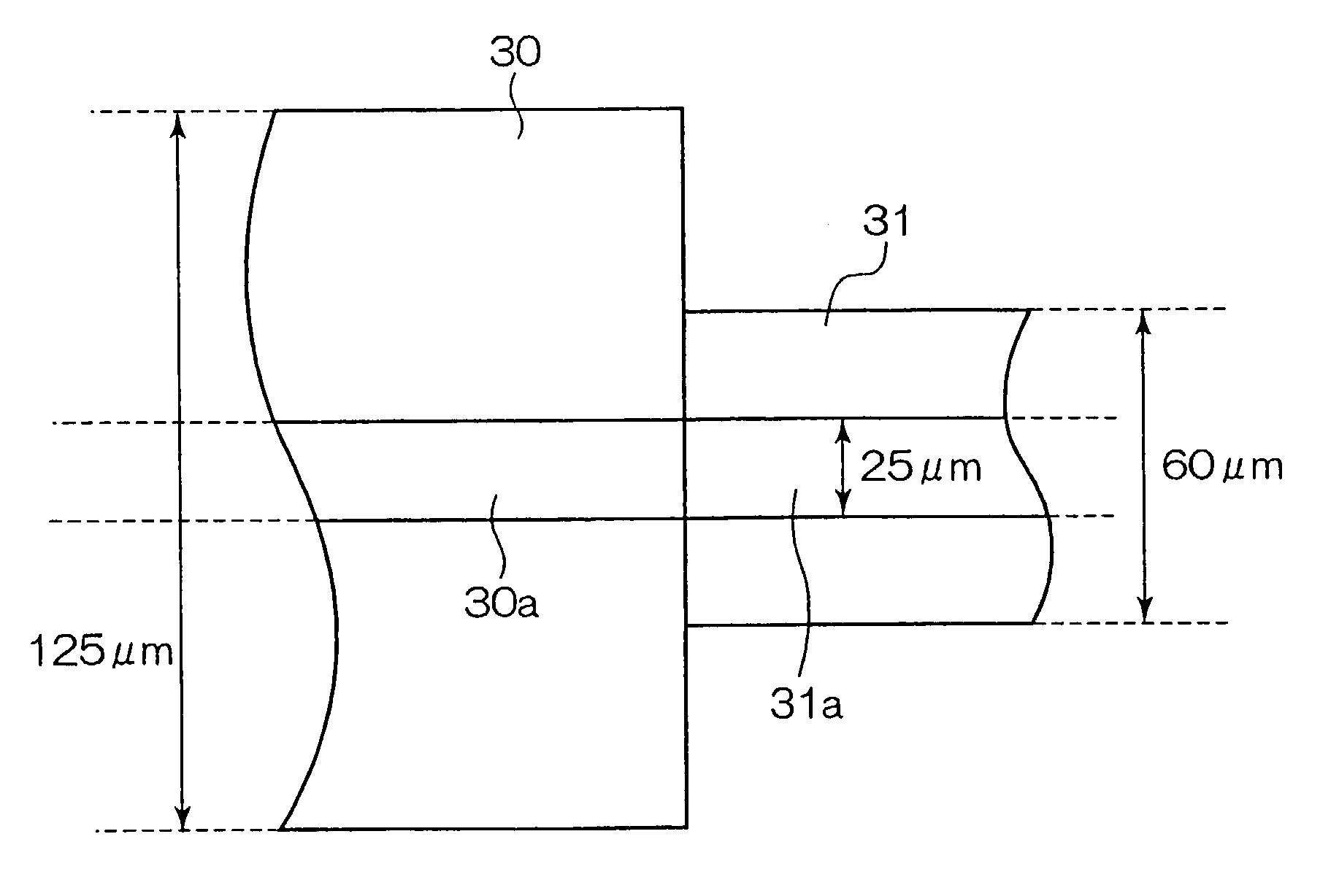
[0199]As shown in FIGS. 36A and 36B, the illumination head 500 is composed of a fiber array light source 506 having a laser light exit section 68 in which the exit ends (emission points) of a number of (e.g., 1,200) optical fibers 30 are arranged in line perpendicularly to the auxiliary sc...


PUM

PropertyMeasurementUnit
wavelengthaaaaaaaaaa
temperaturesaaaaaaaaaa
deformation temperatureaaaaaaaaaa

Abstract

A laser annealer has a laser light source with at least one GaN-type semiconductor laser and is configured so as to form emission points that emit laser beams having a wavelength of 350 to 450 nm, and a scanning device for scanning an annealing surface with the laser beams. The laser annealer may have a spatial light modulator for modulating the laser beams, and in which pixel portions whose light modulating states change in accordance with control signals are arranged on a substrate. The invention is applied to a laser thin-film forming apparatus. The apparatus has a laser source that has at least one semiconductor laser and is configured so as to form emission points, and an optical system for focusing laser beams into a single beam in the width direction of a substrate.

Description

CROSS-REFERENCE TO RELATED APPLICATIONS[0001]This application claims priority under 35 USC 119 from Japanese Patent Applications No. 2002-167279, No. 2002-167280, No. 2002-167281 and No. 2002-198248, the disclosures of which are incorporated by reference herein.BACKGROUND OF THE INVENTION[0002]1. Technical Field[0003]The present invention relates to a laser annealer and a laser thin-film forming apparatus. Particularly, the invention relates to a laser annealer using a GaN (gallium nitride) type semiconductor laser as a light source and a laser thin-film forming apparatus for depositing a thin-film on a substrate that is accommodated in a closed space using products obtained by applying a laser beam to a material gas or a solid material in the closed space and causing a decomposing or synthesizing reaction.[0004]2. Description of the Related Art[0005]From the viewpoint of reduction in the size, weight, and cost of flat panel displays such as liquid crystal displays (LCDs) and organi...

Claims


Application Information

Patent Timeline
Patent Type & Authority Patents(United States)
IPC IPC(8): B23K26/00B23K26/06C23C14/28C23C16/48H01L21/203
CPCB23K26/0604C23C16/483C23C14/28B23K26/0608H01L21/324
Inventor ISHIKAWA, HIROMIHARADA, AKINORINAGANO, KAZUHIKOOKAZAKI, YOJIFUJII, TAKESHIYAMANAKA, HIDEOYAMAKAWA, HIROMITSU
Owner FUJIFILM HLDG CORP
Why Eureka
Try Eureka