

Method of making diode structures
- Summary
- Abstract
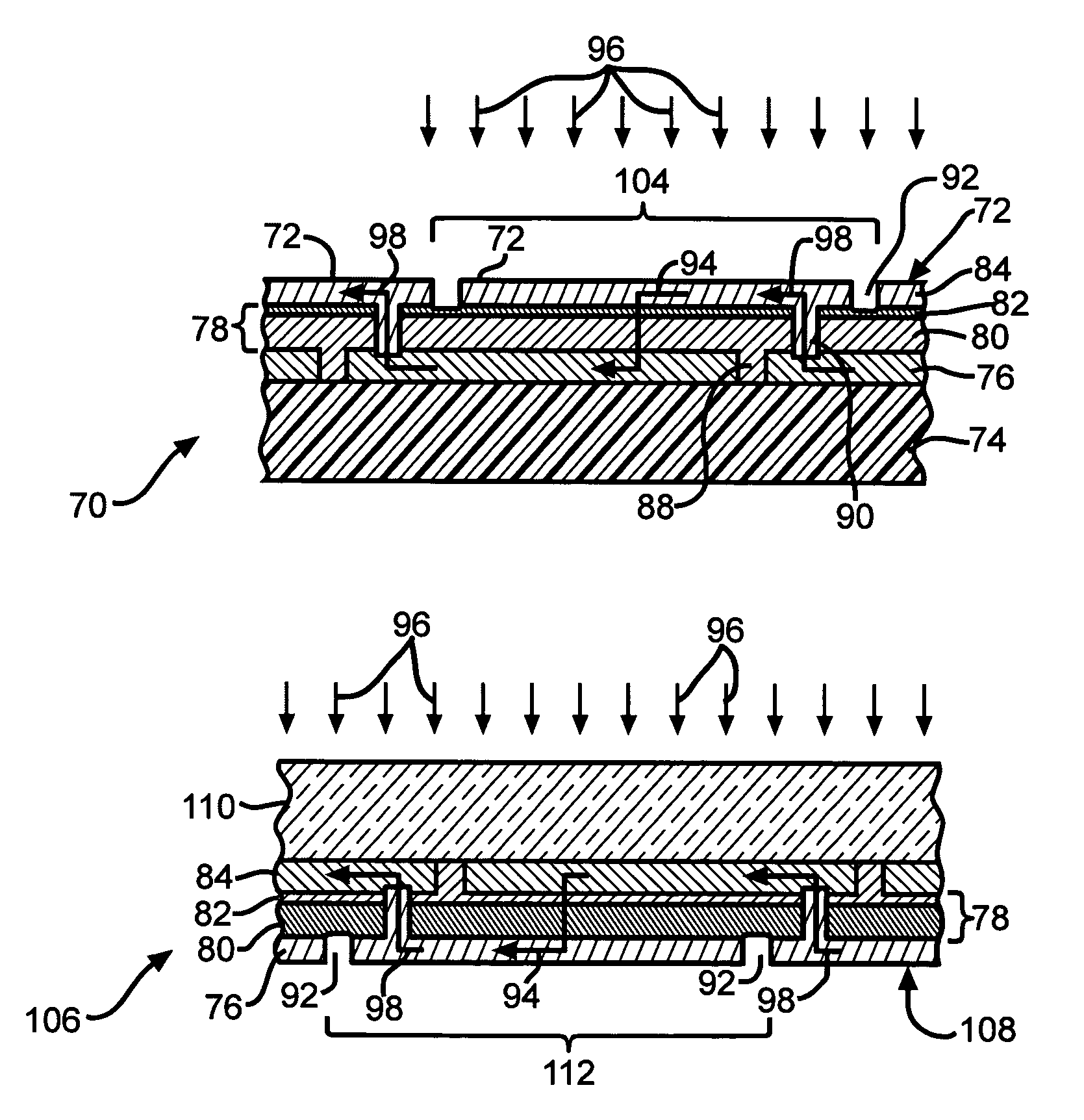
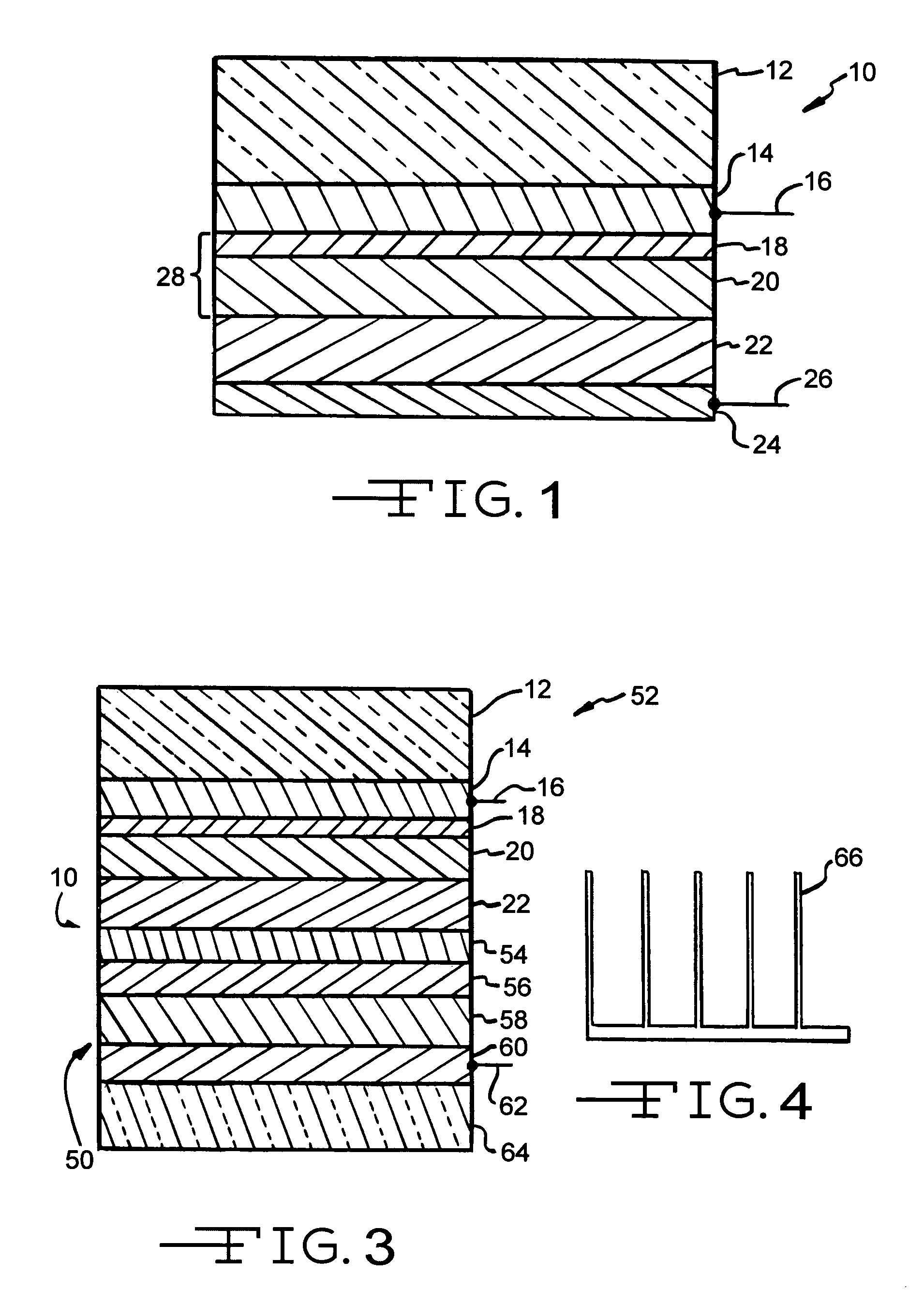
- Description
- Claims
- Application Information
AI Technical Summary
Benefits of technology
Problems solved by technology
Method used
Image

Examples
example i
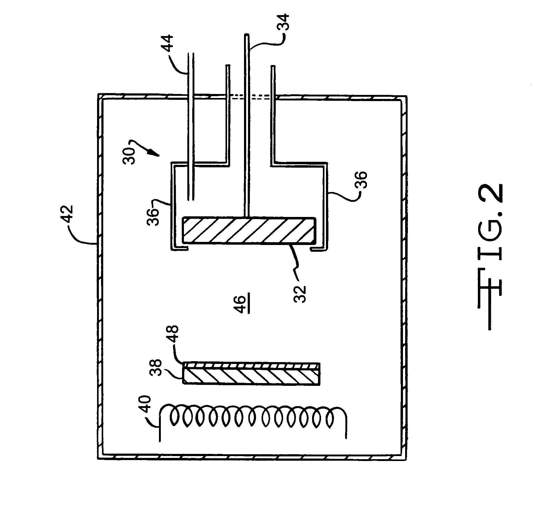
[0042]A thin-film photovoltaic cell was made using the method of the invention. First, a substrate layer of aluminosilicate glass was coated with a ZnO layer doped with aluminum using an RF sputtering process. Then, RF sputtering was used to add an n-type layer of CdS and a p-type layer of CdTe at a temperature of about 250 degrees C. The two-inch sputter sources were commercially available pressed and sintered targets with purity of 99.99% to 99.999%. A vapor CdCl2 treatment at 385–390 C was used before contacting with the application of the back electrode layer. Finally, a back electrode layer of Cu / Au was applied using a thermal evaporation process. No etching or rinse was used at any point after the initial glass cleaning. The RF (or pulsed DC) sputtering was carried out in a chamber assembled from a six-way stainless steel, copper gasketed cross with a two-inch planar magnetron mounted horizontally in one arm. The magnetron used an unbalanced magnetic field configuration. The b...
example ii
[0043]The solar cell produced in Example I was tested for conversion efficiency, defined as the amount of electric energy produced as a percentage of the incident solar energy. When tested for conversion efficiency, the result was a conversion efficiency of about 14 percent, as measured using an air mass 1.5 solar simulator with intensity and spectrum equivalent to one sun at air mass 1.5 (sunlight after passing through 1.5 times the thickness of the earth's atmosphere). The improved performance over conventional solar cells was primarily due to higher current through the front transparent electrode layer 14. The ZnO-based photovoltaic cell had a short-circuit current per unit area of JSC=23.6 mA / cm2 vs. 20.7 mA / cm2 for a similar sputtered 12.6% cell on a commercial tin-oxide coated (Pilkington, Tec-7) soda-lime glass substrate. Other parameters were fill factor, FF=73.25% and open-circuit voltage, VOC=814 mV, for an NREL (National Renewable Energy Laboratory) verified efficiency of...
example iii
[0044]The front transparent electrode layer of the photovoltaic cell produced in Example I was tested for electrical sheet resistance using a four-point probe tester, and measured at 2 ohms per square with about 90 percent transparency. In contrast, conventional transparent electrode layers of doped tin oxide typically have electrical sheet resistance greater than about 7 ohms per square, and they transmit no more than about 80 percent of the visible light.
PUM
 Abstract
Description
Claims
Application Information