Semiconductor light-emitting device and method for fabricating the same

Inactive Publication Date: 2007-01-30
PANASONIC CORP
View PDF12 Cites 5 Cited by
  • Summary
  • Abstract
  • Description
  • Claims
  • Application Information

AI Technical Summary

Benefits of technology

[0012]It is therefore an object of the present invention to solve the conventional problems and thereby improve the adhesion of a current blocking layer provided in a semiconductor light-emitting device composed of a Group III–V nitride semiconductor, while reducing a pinhole density therein.
[0014]In the semiconductor light-emitting device according to the present invention, the dielectric material obtained by replacing some of the nitrogen atoms composing the semiconductor layer composed of the group III–V nitride is used for the current blocking layer so that the current blocking layer is formed integrally with the semiconductor layer. This resolves the problem of the current blocking layer associated with the adhesion thereof to the semiconductor layer and significantly reduces the pinhole density.
[0016]In the arrangement, the composition of oxygen in the semiconductor layer increases gradually with distance from the inside of the semiconductor layer toward the outside thereof so that the refractive index difference between the semiconductor layer and the current blocking layer changes continuously. This allows an increase in the width of an opening in the current blocking layer for effecting single lateral mode confinement if the semiconductor light-emitting device is, e.g., a laser device and permits easy optimization of the laser structure.
[0021]In accordance with the method for fabricating a semiconductor light-emitting device according to the present invention, the semiconductor layer composed of a Group III–V nitride is formed on the active layer and the mask film is formed selectively thereon. The semiconductor layer is then oxidized by using the formed mask film to form the current blocking layer composed of a dielectric material obtained by replacing some of the nitrogen atoms composing the semiconductor layer with oxygen atoms. This prevents a problem associated with the adhesion between the current blocking layer and the semiconductor layer. Since some of the nitrogen atoms composing the semiconductor layer have been replaced with oxygen atoms which are larger in atomic radius than the nitrogen atoms, the volume of the semiconductor layer is increased so that a pinhole density in the current blocking layer is reduced significantly.

Problems solved by technology

Each of the silicon dioxide and silicon nitride has the problems of poor adhesion to a group III–V nitride semiconductor, a high density of small holes, i.e., a high pinhole density, and the like.
This causes the problem of an increased DC resistance component in a current path.
If the stripe width is reduced excessively, the DC resistance component is increased disadvantageously as described above.
Because of the large confinement efficiency, the light emitting point of the laser light may displace at a high power output and the configuration of the spot is liable to change when the light is confined in the cavity under this condition.
For this reason, the design for optimizing the laser structure is rather difficult in equipment requiring accurate control of the light emitting point and the spot configuration, such as an optical laser disk device.

Method used


Image

  • Semiconductor light-emitting device and method for fabricating the same
  • Semiconductor light-emitting device and method for fabricating the same
  • Semiconductor light-emitting device and method for fabricating the same

Examples


embodiment 1

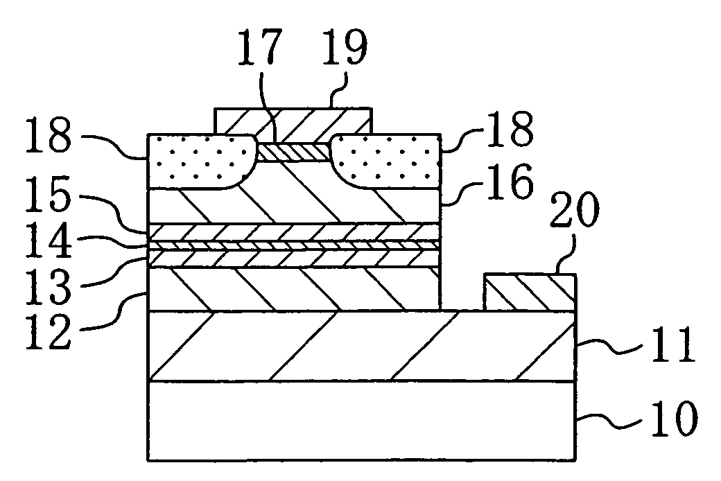
[0036]A first embodiment of the present invention will be described with reference to the drawings.

[0037]FIG. 1 shows a cross-sectional structure of a semiconductor laser device according to the first embodiment.

[0038]The semiconductor laser device shown in FIG. 1 has a double heterostructure including cladding layers composed of an aluminum gallium nitride (AlGaN) having a relatively large band gap and a quantum well layer and the like composed of any of a gallium nitride (GaN), a gallium indium nitride (GaInN) and a combination thereof each having a band gap smaller than that of the cladding layers, which are sandwiched between the cladding layers. A description will be given herein below to the case where a single quantum well separate confinement heterostructure (SQW-SCH) is used.

[0039]As shown in FIG. 1, an n-type buffer layer 11 composed of n-type GaN with a thickness of about 2 μm, an n-type cladding layer 12 composed of n-type Al0.15Ga0.85N with a thickness of about 1 μm, an...

embodiment 2

[0071]A second embodiment of the present invention will be described herein below with reference to the drawings.

[0072]FIG. 8 shows a cross-sectional structure of a semiconductor laser device according to the second embodiment.

[0073]In contrast to the first embodiment which uses insulating sapphire to compose the substrate 10 on which the epitaxial layer is grown, the second embodiment uses, to compose a substrate 30, any of an n-type gallium nitride (GaN), an n-type aluminum gallium nitride (AlGaN), and an n-type silicon carbide (SiC) each having conductivity and close in lattice constant to a Group III nitride semiconductor, as shown in FIG. 8.

[0074]As shown in FIG. 8, an n-type buffer layer 31 composed of n-type GaN with a thickness of about 2 μm, an n-type cladding layer 32 composed of n-type Al0.15Ga0.85N with a thickness of about 1 μm, an n-type optical confinement layer 33 composed of n-type GaN with a thickness of about 0.1 μm, a single quantum well active layer 34 composed ...

embodiment 3

[0088]A third embodiment of the present invention will be described herein below with reference to the drawings.

[0089]FIG. 10 shows a cross-sectional structure of a semiconductor laser device according to the third embodiment.

[0090]A structure according to the third embodiment is obtainable by further improving the light confining efficiency of the ridge structure of the semiconductor laser device described in the second embodiment.

[0091]As shown in FIG. 10, an n-type buffer layer 51 composed of n-type GaN with a thickness of about 2 μm, an n-type cladding layer 52 composed of n-type Al0.15Ga0.85N with a thickness of about 1 μm, an n-type optical confinement layer 53 composed of n-type GaN with a thickness of about 0.1 μm, a single quantum well active layer 54 composed of undoped Ga0.8In0.2N with a thickness of about 5 μnm, a p-type optical confinement layer 55 composed of p-type GaN with a thickness of about 0.1 μm, a p-type cladding layer 56 composed of p-type Al0.15Ga0.85N with a...


PUM


Abstract

An n-type buffer layer composed of n-type GaN, an n-type cladding layer composed of n-type AlGaN, an n-type optical confinement layer composed of n-type GaN, a single quantum well active layer composed of undoped GaInN, a p-type optical confinement layer composed of p-type GaN, a p-type cladding layer composed of p-type AlGaN, and a p-type contact layer composed of p-type GaN are formed on a substrate composed of sapphire. A current blocking layer formed in an upper portion of the p-type cladding layer and on both sides of the p-type contact layer to define a ridge portion is composed of a dielectric material obtained by replacing some of nitrogen atoms composing a Group III–V nitride semiconductor with oxygen atoms.

Description

[0001]This application is a divisional of Application Ser. No. 10 / 243,711 filed Sep. 16, 2002, now U.S. Pat. No. 6,746,948.BACKGROUND OF THE INVENTION[0002]The present invention relates to a semiconductor light-emitting device composed of a Group III–V nitride semiconductor which is capable of outputting light ranging in color from blue to ultraviolet and to a method for fabricating the same.[0003]In recent years, semiconductor light-emitting devices each using a Group III–V nitride semiconductor represented by a general formula: BxAlyGa1-x-y-zInzN (where x, y, and z satisfy 0≦x≦1, 0≦y≦1, 0≦z≦1, x+y+z=1), i.e., a light-emitting diode device and a semiconductor laser device have been developed vigorously as light sources for emitting light ranging in color from blue to ultraviolet.[0004]Referring to the drawings, a conventional semiconductor light-emitting device composed of a Group III–V nitride semiconductor will be described.[0005]As shown in FIG. 13, an n-type contact layer 102 c...

Claims


Application Information

Patent Timeline
IPC IPC(8): H01L29/732H01L31/072H01L33/14H01L33/32H01S5/22H01S5/343
CPCB82Y20/00H01S5/34333H01L33/145H01S5/2214H01S5/2215H01L33/32
Inventor UEDA, DAISUKETAKIGAWA, SHINICHI
Owner PANASONIC CORP
Why Eureka
Try Eureka