Three-dimensional stacked semiconductor package device with bent and flat leads and method of making same

a semiconductor and package technology, applied in semiconductor devices, semiconductor/solid-state device details, electrical apparatus, etc., can solve the problems of defect density control, optical system resolution limit, and limited availability of processing material and equipment, so as to improve the efficiency of manufacturing and reduce the size of features. , the effect of convenient manufacturing

Inactive Publication Date: 2007-03-13
BRIDGE SEMICON
View PDF92 Cites 90 Cited by
  • Summary
  • Abstract
  • Description
  • Claims
  • Application Information

AI Technical Summary

Benefits of technology

[0040]An advantage of the stacked device of the present invention is that it is reliable, cost-effective, easily manufacturable, compact, and can be directly mounted on a printed circuit board. Another advantage is that the stacked device can use semiconductor package devices with flat leads above the first semiconductor package device which simplifies manufacturing. Another advantage is that the stacked device can include solder balls as conductive bonds for vertical electrical interconnects between the leads and near the insulative housings which reduces space. Another advantage is that the stacked device can accommodate chips with varying sizes and thickness while maintaining reliable vertical electrical interconnects between the chips. Another advantage is that the stacked device need not include wire bonds or TAB leads. Another advantage is that the stacked device can be manufactured using first and second semiconductor package devices that are essentially identical to one another except for the leads and additional semiconductor package devices that are essentially identical to the second semiconductor package device. Another advantage is that the stacked device can be manufactured using low temperature processes which reduces stress and improves reliability. A further advantage is that the stacked device can be manufactured using well-controlled processes which can be easily implemented by circuit board, lead frame and tape manufacturers. Still another advantage is that the stacked device can be manufactured using materials that are compatible with copper chip and lead-free environmental requirements.

Problems solved by technology

However, significant obstacles to further reduction in feature size are being encountered.
These obstacles include defect density control, optical system resolution limits, and availability of processing material and equipment.
In addition, flip-chip bonding requires minimal mounting area and weight which results in overall cost saving since no extra packaging and less circuit board space are used.
While flip-chip technology has tremendous advantages over wire bonding and TAB, its cost and technical limitations are significant.
For instance, the cost of forming bumps on the pads is significant.
An adhesive is normally underfilled between the chip and the support circuit to reduce stress on the solder joints due to thermal mismatch between the chip and the support circuit, and the underfilling process increases both manufacturing complexity and cost.
Further, the solder is typically a tin-lead alloy and lead-based materials are becoming far less popular due to environmental concerns over disposing of toxic materials and leaching of toxic materials into ground water supplies.
Thus, none of these conventional connection techniques are entirely satisfactory.
Conventional single-chip packages typically have an area (or footprint) that is many times larger than the area of the chip, causing the printed circuit board to have excessively large area relative to the chips.
However, as chip speeds increase, it becomes critical to position the chips close together since excessive signal transmission distance deteriorates signal integrity and propagation times. Other considerations such as manufacturing cost, reliability, heat transfer, moisture resistance, mounting and interconnect standardization, testability, and quality control have also become focal points of chip packaging.
Although these packages provide certain advantages, further size reduction and performance enhancement with these packages has been difficult to obtain due to physical dimension, design and manufacturing constraints.
However, since multichip modules utilize a planar interconnection substrate as the base, their effectiveness in packaging density is limited.
The single-chip packages also have long extended leads and associated wire bonds that limit electrical performance.
The solder balls require large amounts of space.
The flexible film is relatively difficult to wrap and bending the wiring layers causes low yields.
The TAB leads for different chips have different shapes and lengths which complicates manufacturing.
Furthermore, the TAB leads are interconnected by applying thermocompression, which also complicates manufacturing.
The wafer process must be modified, and aligning the sidewalls and forming the routing lines on the leads is difficult.
The wafer stacks are difficult to separate for repairs and too large for many applications.
Another drawback with many conventional three-dimensional packages is that the vertical interconnects lack the flexibility to accommodate thickness variations of the stacked assemblies.
As a result, vertical interconnects with fixed heights cannot adequately accommodate these thickness variations, and suffer from disoriented, cracked and open connections, high mechanical stress and reliability problems.
In summary, conventional three-dimensional packages suffer from numerous deficiencies including large area requirements, inflexible vertical interconnects, limited electrical performance, poor structural strength and low reliability.
Moreover, conventional three-dimensional packages are often manufactured by complicated processes that are impractical for volume production, and too difficult and costly to develop.

Method used


Image

  • Three-dimensional stacked semiconductor package device with bent and flat leads and method of making same
  • Three-dimensional stacked semiconductor package device with bent and flat leads and method of making same
  • Three-dimensional stacked semiconductor package device with bent and flat leads and method of making same

Examples


Embodiment Construction

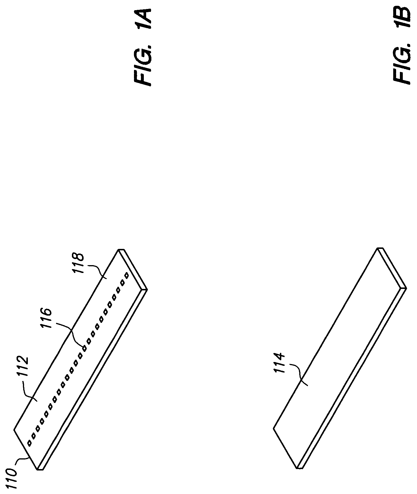
[0068]FIGS. 1A–18A and 1B–18B are top and bottom perspective views, respectively, of a method of making a three-dimensional stacked semiconductor package device in accordance with an embodiment of the present invention.

[0069]FIGS. 1A and 1B are top and bottom perspective views, respectively, of semiconductor chip 110 which is an integrated circuit in which various transistors, circuits, interconnect lines and the like are formed (not shown). Chip 110 includes opposing major surfaces 112 and 114 and has a thickness of 200 microns between these surfaces. Surface 112 is an upper surface, and surface 114 is a lower surface. Surface 112 is the active surface and includes conductive pads 116 arranged in a single row and passivation layer 118. Pads 116 are substantially aligned with passivation layer 118 so that surface 112 is essentially flat. Alternatively, if desired, pads 116 can extend above or be recessed below passivation layer 118. Pads 116 provide bonding sites to electrically cou...


PUM


Abstract

A three-dimensional stacked semiconductor package device includes first and second semiconductor package devices and a conductive bond. The first device includes a first insulative housing, a first semiconductor chip and a first lead that is bent outside the first insulative housing. The second device includes a second insulative housing, a second semiconductor chip and a second lead that is flat outside the second insulative housing. The conductive bond contacts and electrically connects the leads.

Description

CROSS-REFERENCE TO RELATED APPLICATIONS[0001]This application is a continuation-in-part of U.S. application Ser. No. 10 / 136,954 filed Apr. 30, 2002 (now U.S. Pat. No. 6,716,670), which is a continuation-in-part of U.S. application Ser. No. 10 / 042,812 filed Jan. 9, 2002, now U.S. Pat. No. 6,891,276 each of which is incorporated by reference.[0002]This application is also a continuation-in-part of U.S. application Ser. No. 10 / 137,494 filed Apr. 30, 2002 (now U.S. Pat. No. 6,744,126), which is a continuation-in-part of U.S. application Ser. No. 10 / 042,812 filed Jan. 9, 2002, now U.S. Pat. No. 6,891,276 each of which is incorporated by reference.BACKGROUND OF THE INVENTION[0003]1. Field of the Invention[0004]The present invention relates to semiconductor packaging, and more particularly to stacked semiconductor package devices and their method of manufacture.[0005]2. Description of the Related Art[0006]In the field of electronic systems, there is a continuous need to increase performanc...

Claims


Application Information

Patent Timeline
Patent Type & Authority Patents(United States)
IPC IPC(8): H01L23/02H01L23/28H01L23/48H01L23/495H01L25/10
CPCH01L23/49555H01L25/105H01L2224/16H01L2225/1029H01L2225/1058H01L2924/09701
Inventor CHIANG, CHENG-LIEN
Owner BRIDGE SEMICON
Why Eureka
Try Eureka