Semiconductor device including two transistors and capacitive part

a technology of capacitive parts and semiconductors, applied in the direction of semiconductor devices, electrical devices, transistors, etc., can solve the problems of deterioration of characteristic properties, decrease of mobility and on-current after prolonged operation, and increase of off-current (leakage current) of polysilicon films, etc., to achieve high driving performance and high reliability

Inactive Publication Date: 2007-04-10
SEMICON ENERGY LAB CO LTD
View PDF27 Cites 20 Cited by
  • Summary
  • Abstract
  • Description
  • Claims
  • Application Information

AI Technical Summary

Benefits of technology

[0014]The present invention was completed in order to overcome the above-mentioned problems. It is an object of the present invention to provide a first TFT of new structure in which the gate electrode overlaps with the LDD region. It is another object of the present invention to provide a second TFT of such structure in which the gate electrode does not overlap with the LDD region. It is further another object of the present invention to provide a technology to produce simultaneously a first TFT of new structure in which the gate electrode overlaps with the LDD region and a second TFT of such structure in which the gate electrode does not overlap with the LDD region. It is still further another object of the present invention to provide an excellent semiconductor device whose circuits are constructed of TFTs with high driving performance and TFTs with high reliability.

Problems solved by technology

Unfortunately, TFTs made of polysilicon film tend to increase in off-current (leakage current).
This leads to a decrease in mobility and on-current after prolonged operation.
A probable reason for this trouble is an increase in channel electric field which gives rise to hot carriers and deteriorates the characteristic properties.
The structure reported in this paper presents difficulties in leaving the gate insulating film highly selectively in the anisotropic etching of film for the side wall.
Therefore, when TFTs of the reported structure are used as switching elements to drive pixel electrodes, they consume more electric power and display anomalous images due to large off-current.

Method used


Image

  • Semiconductor device including two transistors and capacitive part
  • Semiconductor device including two transistors and capacitive part
  • Semiconductor device including two transistors and capacitive part

Examples


embodiment 1

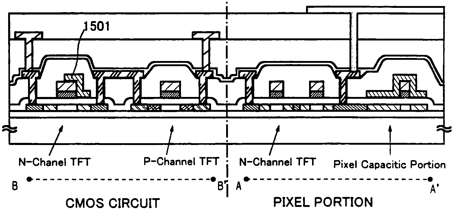
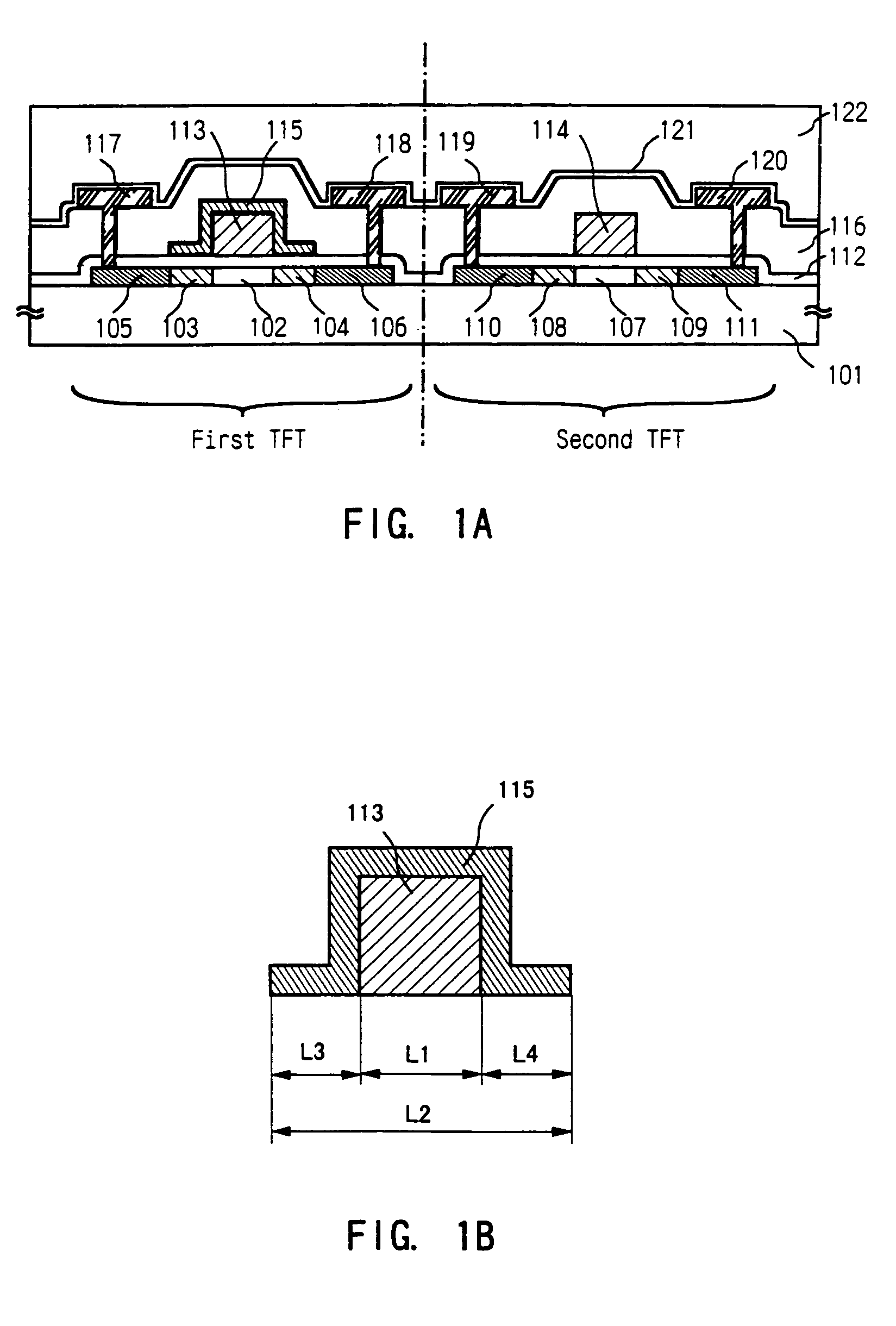
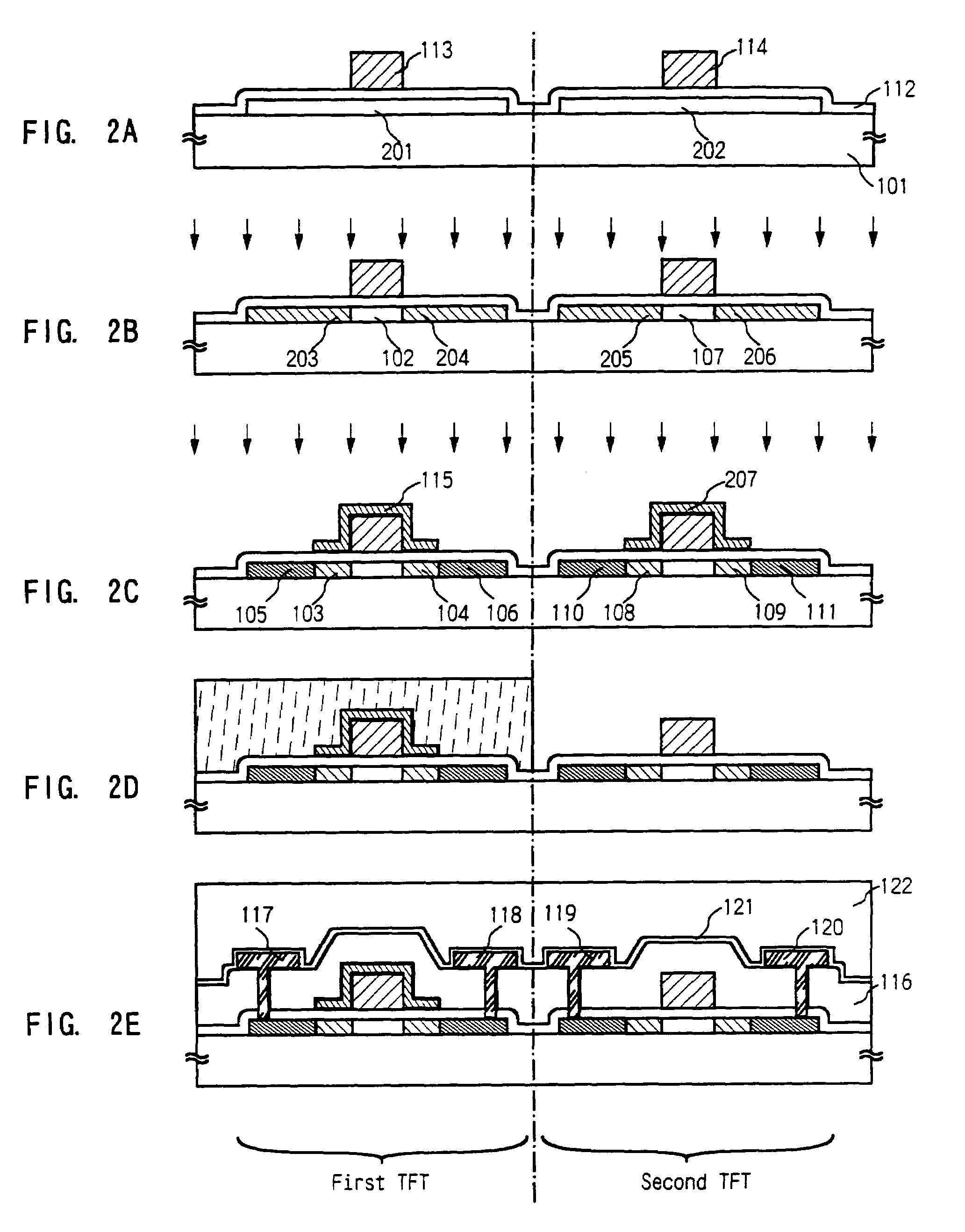
[0080]This embodiment demonstrates the application of the present invention to liquid crystal display units. The process in this embodiment is designed to produce the pixel and the CMOS circuit (as the drive circuit) as shown in FIGS. 3 and 4.

[0081]The substrate 301 was prepared from alkali-free glass typified by 1737 glass from Corning Glass Works. An underlying film 302 of silicon oxide (200 nm thick) was formed on the surface of the substrate 301 on which TFT was to be formed. The underlying film 302 may optionally be coated with silicon nitride film.

[0082]On the underlying film 302 was formed an amorphous silicon film (50 nm thick) by plasma CVD. The amorphous silicon film was heated (preferably at 400–500° C. depending on its hydrogen content) for dehydrogenation so that the hydrogen content was reduced to 5 atomic % or less. The amorphous silicon film was converted into crystalline silicon film by crystallization.

[0083]The process for crystallization may be accomplished by any...

embodiment 2

[0116]This embodiment differs from Embodiment 1 in that the crystalline semiconductor film as the semiconductor layer is formed by thermal crystallization with the aid of a catalytic element. This step should preferably be carried out by using the technology disclosed in Japanese Patent Laid-open No. 130652 / 1995 and 78329 / 1996.

[0117]The technology disclosed in Japanese Patent Laid-open No. 130652 / 1995 was applied to the present invention as shown in FIG. 7. On the silicon substrate 601 was formed sequentially the silicon oxide film 602 and the amorphous silicon film 603. Further, the nickel-containing layer 604 was formed by coating with a nickel acetate solution containing 10 ppm of nickel (by weight). (FIG. 7(A))

[0118]Dehydration at 500° C. for 1 hour and heat treatment at 500–650° C. for 4–12 hours (for example, at 550° C. for 8 hours) were carried out so as to form the crystalline silicon film 605. The resulting crystalline silicon film 605 was superior in crystallinity. (FIG. 7...

embodiment 3

[0125]This embodiment demonstrates the procedure to form the semiconductor layer used in Embodiment 1. In this procedure, an amorphous semiconductor film is formed first and then it is crystallized with the aid of the above-mentioned catalytic element, which is finally removed from the crystalline semiconductor film. The procedure in this embodiment is based on the technology disclosed in Japanese Patent Laid-open No. 135468 / 1998 and 135469 / 1998.

[0126]This technology is concerned with the removal of the catalytic element (used for crystallization of the amorphous semiconductor film) by gettering after crystallization. This technology makes it possible to reduce the concentration of the catalytic element in the crystalline semiconductor film down to 1×10¹⁷ atms / cm3, preferably 1×10¹⁶ atms / cm3.

[0127]This embodiment is explained with reference to FIG. 9. The substrate is alkali-free glass typified by 1737 glass from Corning Glass Works. FIG. 9(A) shows the underlying film 802 and the c...


PUM


Abstract

An object of the present invention is to provide a TFT of new structure in which the gate electrode overlaps with the LDD region and a TFT of such structure in which the gate electrode does not overlap with the LDD region. The TFT is made from crystalline semiconductor film and is highly reliable.The TFT of crystalline semiconductor film has the gate electrode formed from a first gate electrode 113 and a second gate electrode in close contact with said first gate electrode and gate insulating film. The LDD is formed by ion doping using said first gate electrode as a mask, and the source-drain region is formed using said second gate electrode as a mask. After that the second gate electrode in the desired region is selectively removed. In this way it is possible to form LDD region which overlaps with the second gate electrode.

Description

[0001]This application is a divisional of U.S. application Ser. No. 10 / 140,424, filed on May 6, 2002, now U.S. Pat. No. 6,803,601 issued Oct. 12, 2004, which is a divisional of U.S. application Ser. No. 09 / 441,258, filed on Nov. 16, 1999, now U.S. Pat. No. 6,420,758 issued Jul. 16, 2002.BACKGROUND OF THE INVENTION[0002]1. Field of the Invention[0003]The present invention relates to a semiconductor device having circuits composed of thin-film transistors. More particularly, the present invention relates to an electro-optical device represented by a liquid-crystal display unit and also to a structure of electronic machines and equipment equipped with such electro-optical devices. The term “semiconductor device” as used in this specification generally denotes any device which functions by utilizing the semiconductor characteristics and hence it embraces said electro-optical devices and electronic machines and equipment equipped with said electro-optical devices.[0004]2. Description of ...

Claims


Application Information

Patent Timeline
Patent Type & Authority Patents(United States)
IPC IPC(8): H01L29/10H01L21/336H01L21/77H01L21/84H01L27/12H01L27/13H01L29/49H01L29/786
CPCH01L29/4908H01L29/66757H01L27/124H01L29/78627H01L27/1255H01L29/78621
Inventor NAKAJIMA, SETSUO
Owner SEMICON ENERGY LAB CO LTD
Why Eureka
Try Eureka