Method of manufacturing a contact interconnection layer containing a metal and nitrogen by atomic layer deposition for deep sub-micron semiconductor technology

a technology of contact interconnection layer and semiconductor technology, applied in the direction of semiconductor/solid-state device details, semiconductor devices, electrical apparatus, etc., can solve the problems of increasing complexity and cost, shrinking interconnection size, and metal wiring, and achieves good step coverage and safe handling

Active Publication Date: 2007-06-26
TAIWAN SEMICON MFG CO LTD
View PDF22 Cites 390 Cited by
  • Summary
  • Abstract
  • Description
  • Claims
  • Application Information

AI Technical Summary

Benefits of technology

[0009]An objective of the present invention is to provide an improved method of forming a interconnect comprised of at least one metal and nitrogen that can be used as a plug with good step coverage in an opening which has a width of about 100 nm or less. It is desirable that the method should employ a precursor compound that is relatively safe to handle.
[0010]A further objective of the present invention is to provide a more cost effective means of forming an interconnect comprised of at least one metal and nitrogen that has a width of about 100 nm or less.
[0011]A still further objective of the present invention is to provide a method of forming an interconnect comprised of at least one metal and nitrogen that has a reduced impurity content.
[0013]These objectives are achieved in a first embodiment by providing a substrate having an exposed conductive layer. A dielectric layer is deposited on the substrate by a CVD or PECVD method. Optionally, an etch stop layer is formed on the substrate before the dielectric layer is deposited. Typically, a photoresist is patterned on the dielectric layer and is used as a mask while the opening is transferred through the dielectric layer with a plasma etch to expose the conductive layer. The photoresist is removed to leave a contact hole or an opening in the dielectric layer that preferably has a width of about 100 nm or less. An ALD method is employed to deposit a composite layer comprised of a plurality of metal nitride monolayers that completely fills the opening and affords good step coverage. Preferably, the metal is Ti or Ta. When forming TiN, chloride contamination may be avoided by using tetrakis(dimethylamido)titanium (TDMAT), tetrakis(diethylamido)titanium (TDEAT), or Ti{OCH(CH3)2}4 as the titanium precursor.

Problems solved by technology

Metal wiring in a device forms vertical and horizontal interconnections that are shrinking in size and increasing in complexity as technology advances to 100 nm ground rules and beyond.
Therefore, at least three deposition steps are employed in plug formation which adds complexity and cost to the device fabrication.
In the case of a contact hole 4 that has a width w of about 100 nm or less, the conventional plug formation process does not adequately fill the contact hole 4.
Note that an opening 8 still exists in contact hole 4 and this space is considered a defect that will degrade the performance of the final device.
While this technique is successful for filling contacts with a diameter in the 130 to 150 nm range, a problem similar to that depicted in FIG. 1 is anticipated for filling holes that have a width of 100 nm or less.
Although nitrates avoid the chloride contamination concern, they are highly flammable and explosive.

Method used


Image

  • Method of manufacturing a contact interconnection layer containing a metal and nitrogen by atomic layer deposition for deep sub-micron semiconductor technology
  • Method of manufacturing a contact interconnection layer containing a metal and nitrogen by atomic layer deposition for deep sub-micron semiconductor technology
  • Method of manufacturing a contact interconnection layer containing a metal and nitrogen by atomic layer deposition for deep sub-micron semiconductor technology

Examples


first embodiment

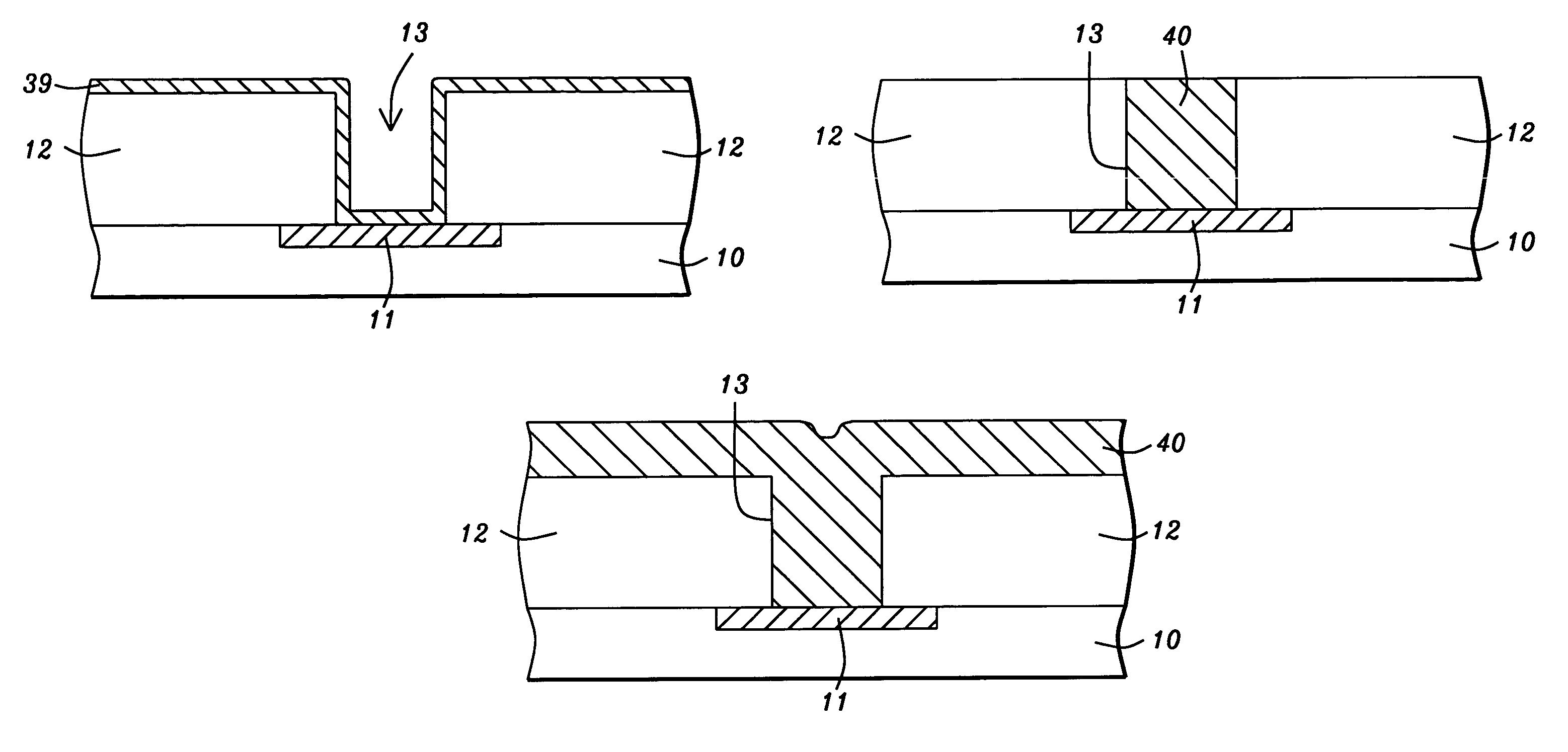
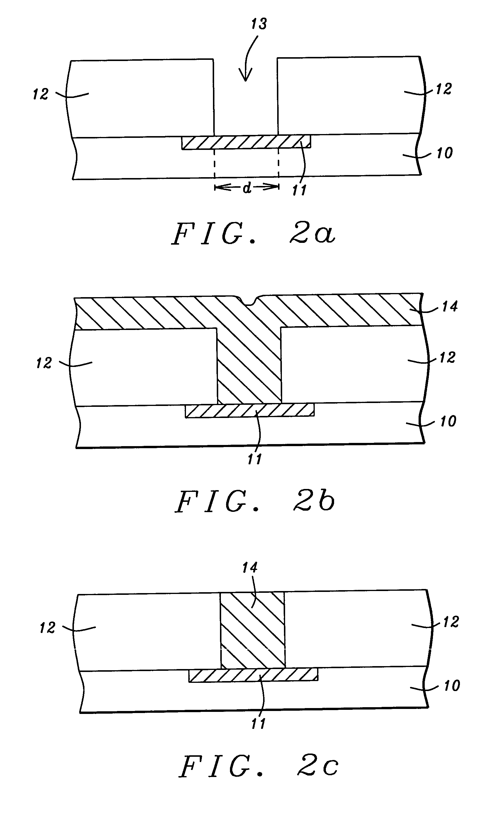
[0023]The present invention is an ALD method that is particularly useful for depositing a plurality of monolayers in an opening formed in a layer on a substrate where the opening is a small contact hole or via that has a width of about 100 nm or less. The plurality of monolayers form a composite layer with two or more elements comprised of at least one metal and nitrogen that is subsequently planarized to fabricate an interconnect or plug. However, the ALD method can also be used to fill other openings such as a trench. In a first embodiment, an ALD method is employed that produces a metal nitride plug with good step coverage, low impurity content, and which does not form any voids.

[0024]Referring to FIG. 2a, a substrate 10 is provided which is typically silicon but may be based on silicon-germanium, gallium arsenide, or silicon-on-insulator technology. The substrate 10 contains a conductive layer 11 that has an exposed upper surface which is coplanar with the top surface of the sub...

second embodiment

[0039]In a second embodiment, the ALD process deposits a composite layer comprised of a plurality of monolayers that include a metal, nitrogen, and a third element that is Si or B. The invention is especially useful for fabricating a composite layer that fills a contact hole or an opening which has a width of about 100 nm or less.

[0040]Referring to FIG. 5, the ALD process of the present invention is depicted in a flow diagram. In step 50, a substrate 10 having a dielectric layer 12 containing an opening 13 as represented in FIG. 4a is positioned on a chuck in an ALD process chamber (not shown) as described in the first embodiment. A vacuum is then applied to the ALD process chamber to remove oxygen and moisture and the temperature is raised to an acceptable level that is required for the ALD deposition. Preferably, the temperature is increased to a range from about 250° C. to 750° C. and the pressure is maintained at about 0.1 Torr to 50 Torr.

[0041]In step 51 which is represented by...

third embodiment

[0055]In another aspect, the composite layer of the third embodiment has the formula M1VM2WSXNZ where v, w, x, and z are fractions between 0 and 1 and which together equal 1, M1 is a first metal, M2 is a second metal, and S is Si or B. For example, the composite layer 40 in FIG. 4e may be further comprised of a fourth element that is a second metal. The composite layer 40 is a plurality of monolayers comprised of one or more monolayers of M1 SN and one or more monolayers of M2SN that are formed by the sequences of steps (51, 52, 53, 54, 55, 56) and (53, 54, 51, 52, 55, 56). During at least one of the cycles that include a step 51, a first metal (M1) gas precursor is flowed into the chamber and during at least one of the cycles that include a step 51, a second metal (M2) gas precursor is flowed into the chamber. For example, Ti{OCH(CH3)2}4 may be flowed into the chamber during one cycle to form a monolayer of TiSiN and TBTDET may be flowed into the chamber during a second cycle to fo...


PUM

PropertyMeasurementUnit
pressureaaaaaaaaaa
temperatureaaaaaaaaaa

Abstract

An atomic layer deposition method is used to deposit a TiN or TiSiN film having a thickness of about 50 nm or less on a substrat. A titanium precursor which is tetrakis(dimethylamido)titanium (TDMAT), tetrakis(diethylamido)titanium (TDEAT), or Ti{OCH(CH3)2}4 avoids halide contamination from a titanium halide precursor and is safer to handle than a titanium nitrate. After a monolayer of the titanium precursor is deposited on a substrate, a nitrogen containing reactant is introduced to form a TiN monolayer which is followed by a second purge. For TiSiN, a silicon source gas is fed into the process chamber after the TiN monolayer formation. The process is repeated several times to produce a composite layer comprised of a plurality of monolayers that fills a contact hole. The ALD method is cost effective and affords an interconnect with lower impurity levels and better step coverage than conventional PECVD or CVD processes.

Description

FIELD OF THE INVENTION[0001]The invention relates to the field of fabricating integrated circuits and in particular to an improved method of forming a plug or interconnect that includes at least one metal and nitrogen with a diameter of less than about 100 nm.BACKGROUND OF THE INVENTION[0002]The formation of contact holes or vias is a critical process during the fabrication of semiconductor devices. Metal wiring in a device forms vertical and horizontal interconnections that are shrinking in size and increasing in complexity as technology advances to 100 nm ground rules and beyond. Current contact interconnect technology that has a 130 to 150 nm minimum feature size is typically based on a tungsten (W) plug that is formed by a chemical vapor deposition (CVD) comprising H2 and WF6 to produce a W layer that has good step coverage on a substrate. However, a Ti / TiN barrier layer is usually required to improve W adhesion to the substrate. Furthermore, a W nucleation layer is necessary to...

Claims


Application Information

Patent Timeline
Patent Type & Authority Patents(United States)
IPC IPC(8): H01L21/44H01L21/285H01L21/768H01L21/8249
CPCH01L21/28562H01L21/76877H01L23/53261H01L2924/0002H01L2924/00
Inventor WU, CHII-MINGTSAI, MING-HSINGHSIEH, CHING-HUASHUE, SHAU-LIN
Owner TAIWAN SEMICON MFG CO LTD
Why Eureka
Try Eureka