

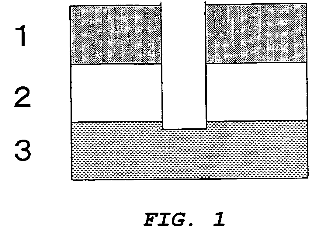
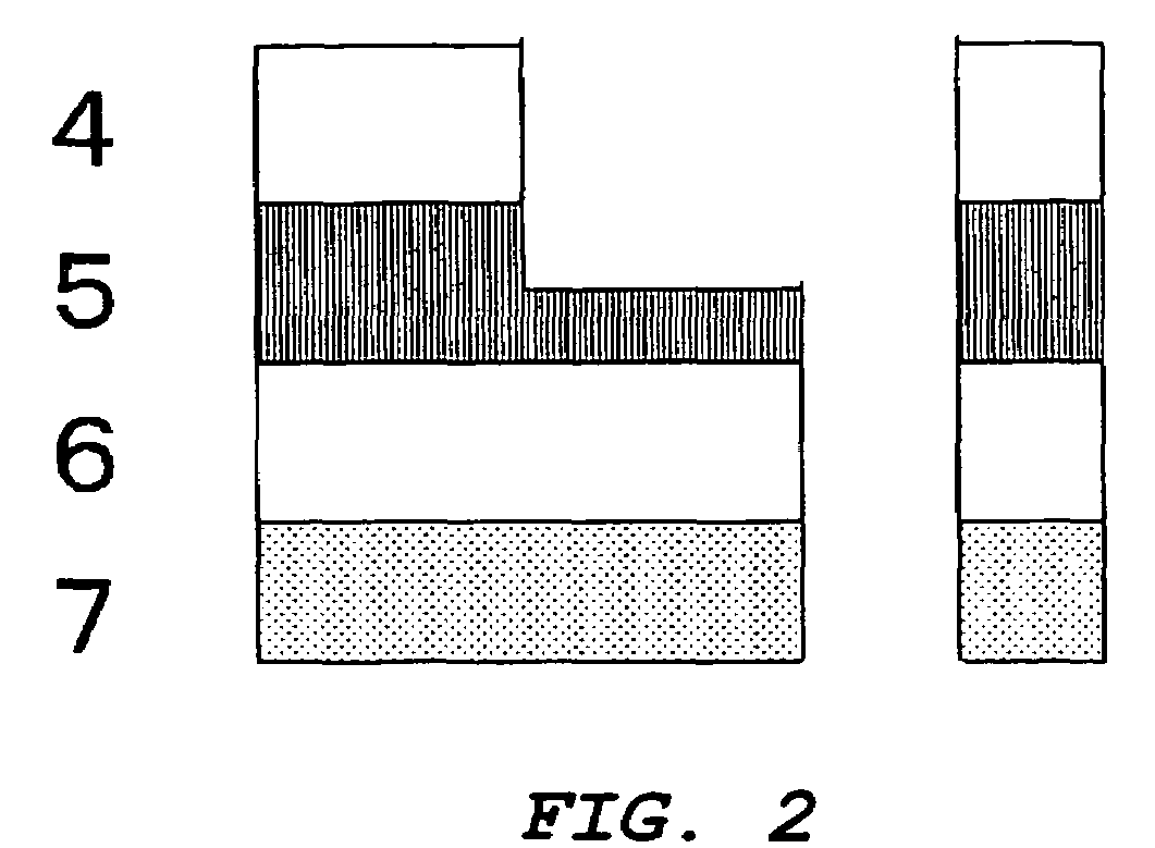
Insulation film
a technology of etching stopper and film, applied in the direction of liquid/solution decomposition chemical coating, superimposed coating process, resistive material coating, etc., can solve the problem of difficult to improve the delay of transmission
- Summary
- Abstract
- Description
- Claims
- Application Information
AI Technical Summary
Benefits of technology
Problems solved by technology
Method used
Image

Examples
synthesis example 1
Synthesis of Organosilicon Polymer
[0100]Poly(phenylsilylene-ethynylene-1,3-phenylene-ethynylene) was dissolved in cyclohexanone to obtain a 15 wt % solution.
[0101]The solution (1) was filtered through a Teflon filter with 0.2 μm pore size to measure the relative dielectric constant of the coating film. The relative dielectric constant was 3.0.
synthesis example 2
Synthesis of Silicon Oxide Interlayer Dielectric Film
[0102]77.04 g of methyltrimethoxysilane, 24.05 g of tetramethoxysilane, and 0.48 g of tetrakis(acetylacetonate)titanium were dissolved in 290 g of propylene glycol mono-propyl ether in a separable quartz flask. The solution was stirred using a three-one motor and the temperature of the liquid was stabilized at 60° C. Next, 84 g of ion exchanged water was added to the solution over one hour. After reacting the mixture for two hours at 60° C., 25 g of acetylacetone was added. The resulting mixtures was reacted for 30 minutes and cooled to room temperature. 149 g of a solution containing methanol and water was removed by evaporation at 50° C.
[0103]The weight average molecular weight of the resulting hydrolysis condensate (either the hydrolyzate or its condensate or both) was 8,900.
example 1
[0104]The etching selection ratio of the etching stopper film made from the organosilicon polymer synthesized in Synthesis Example 1 was evaluated using the above silicon oxide interlayer dielectric film polycarbosilane synthesized in Synthesis Example 2 as an insulating film. An etching apparatus Unity II (manufactured by Tokyo Electron Ltd.) was used under the etching conditions shown in Table 1. The results of the etching selection ratio are shown in Table 1.
[0105]
TABLE 1EtchingconditionsABCDEtching gasC4F8 / Ar / N2C4F8 / ArCF4 / Ar / N2CF4 / ArPressure 10 Pa 10 Pa 10 Pa 10 PaEtching time 20 seconds 20 seconds 20 seconds 20 secondsEtching6.05.86.37.8selection ratio
[0106]A coating film (interlayer dielectric film material) for semiconductor with only minimal damages produced by the etching process can be obtained by using the etching stopper or hard mask made from the organosilicon polymer having a relative dielectric constant of 4 or less of the present invention. In addition, excellent pre...
PUM
| Property | Measurement | Unit |
|---|---|---|
| thickness | aaaaa | aaaaa |
| relative dielectric constant | aaaaa | aaaaa |
| dielectric constant | aaaaa | aaaaa |
Abstract
Description
Claims
Application Information