

Method for manufacturing a potassium niobate deposited body
a technology of potassium niobate and deposited bodies, which is applied in the direction of conductive pattern formation, device material selection, generators/motors, etc., can solve the problem of not having a technology known to date to form a potassium niobate single phase thin film on a substrate of a large surface area, and achieve excellent crystallinity
- Summary
- Abstract
- Description
- Claims
- Application Information
AI Technical Summary
Benefits of technology
Problems solved by technology
Method used
Image

Examples
first embodiment example
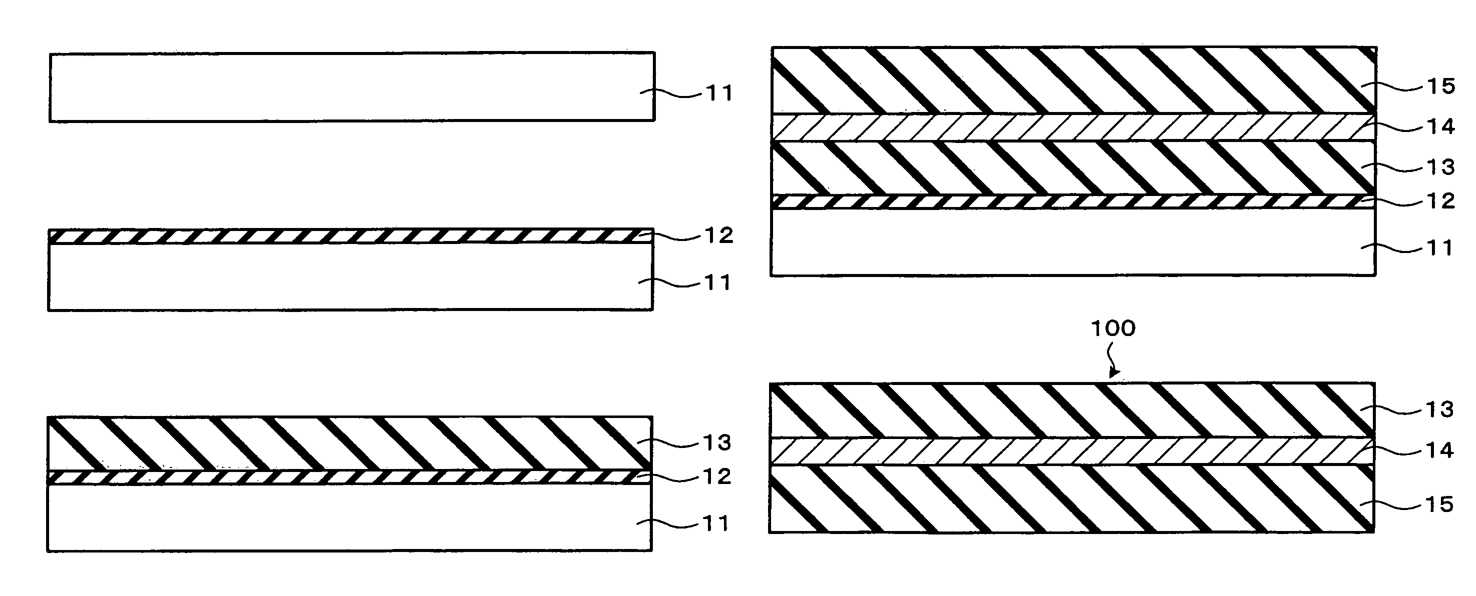
[0096](1) First Embodiment Example
[0097]A potassium niobate deposited body was formed by the following method. In this embodiment example, a polycrystal potassium niobate layer of a single phase could be obtained.
[0098]First, a sapphire single crystal substrate was degreased and washed through soaking the sapphire single crystal substrate in an organic solvent with an ultrasonic washing machine. As the organic solvent, a 1:1 mixed solution of ethyl alcohol and acetone was used. After loading the sapphire single crystal substrate that had been degreased and washed onto a substrate holder, it was introduced together with the substrate holder in a vacuum apparatus whose back pressure at room temperature was 1×10⁻⁸ Torr, oxygen gas was introduced such the oxygen partial pressure became 5×10⁻⁵ Torr, and then the substrate was heated to elevate its temperature up to 400° C. at a rate of 20° C. / minute with an infrared ray lamp.
[0099]Next, a pulsed beam of KrF excimer laser (with a waveleng...
second embodiment example
[0104](2) Second Embodiment Example
[0105]A potassium niobate deposited body was formed by the following method. In this embodiment example, a single crystal potassium niobate layer could be obtained.
[0106]First, a sapphire single crystal substrate was degreased and washed through soaking the sapphire single crystal substrate in an organic solvent with an ultrasonic washing machine. As the organic solvent, a 1:1 mixed solution of ethyl alcohol and acetone was used. After loading the sapphire single crystal substrate that had been degreased and washed onto a substrate holder, it was introduced together with the substrate holder in a vacuum apparatus whose back pressure at room temperature was 1×10⁻⁸ Torr, oxygen gas was introduced such the oxygen partial pressure became 5×10⁻⁵ Torr, and then the substrate was heated to elevate its temperature up to 400° C. at a rate of 20° C. / minute with an infrared ray lamp. At this time, as shown in FIG. 3(A), in a pattern obtained by the reflection...
first example
[0136]4.1 First Example
[0137]FIG. 9 is a block diagram showing an electrical structure of an electronic circuit in accordance with an embodiment of the present invention. It is noted that the electronic circuit in FIG. 9 is a circuit that is provided inside a cellular phone 1000 shown in FIG. 10, for example. FIG. 10 is a perspective view showing an example of the external appearance of the cellular phone which is shown here as one example of an electronic apparatus in accordance with an embodiment of the present invention. The cellular phone 1000 shown in FIG. 10 consists of an antenna 101, a receiver 102, a transmitter 103, a liquid crystal display 104, operating buttons 105, and the like.
[0138]The electronic circuit shown in FIG. 9 has the basic structure of an electronic circuit provided inside the cellular phone 1000, and is equipped with a transmitter 80, a transmission signal processing circuit 81, a transmission mixer 82, a transmission filter 83, a transmission power amplif...
PUM
| Property | Measurement | Unit |
|---|---|---|
| tilt angle | aaaaa | aaaaa |
| tilt angle | aaaaa | aaaaa |
| thickness | aaaaa | aaaaa |
Abstract
Description
Claims
Application Information