Solar cell and method of manufacture

a technology of solar cells and manufacturing methods, applied in the field of solar cells, can solve the problems of limiting the efficiency of silicon photovoltaic cells in directly converting solar energy to electricity to less than 30%, preventing the commercialization of ibc solar cells, and the process is not cost effective for conventional low-cost, flat-plate solar panels. achieve the effect of less expensive and ready-to-manufactur

Active Publication Date: 2008-03-04
MAXEON SOLAR PTE LTD +1
View PDF10 Cites 413 Cited by
  • Summary
  • Abstract
  • Description
  • Claims
  • Application Information

AI Technical Summary

Benefits of technology

[0005]In accordance with the invention, a solar cell structure is provided which can be readily manufact...

Problems solved by technology

These and other losses limit the efficiency of silicon photovoltaic cells in directly converting solar energy to electricity to less than 30%.
While interdigitated back-contact (IBC) solar cells have been fabricated, cost considerations have prevented the IBC solar cell from being commercialized.
This fabrication process is capable of producing high efficiency solar cells, but the process is not cost effective for application in conventional low-cost, ...

Method used


Image

  • Solar cell and method of manufacture
  • Solar cell and method of manufacture
  • Solar cell and method of manufacture

Examples


Embodiment Construction

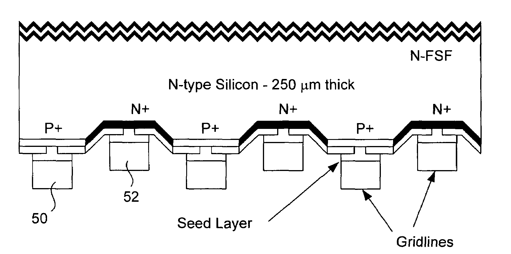
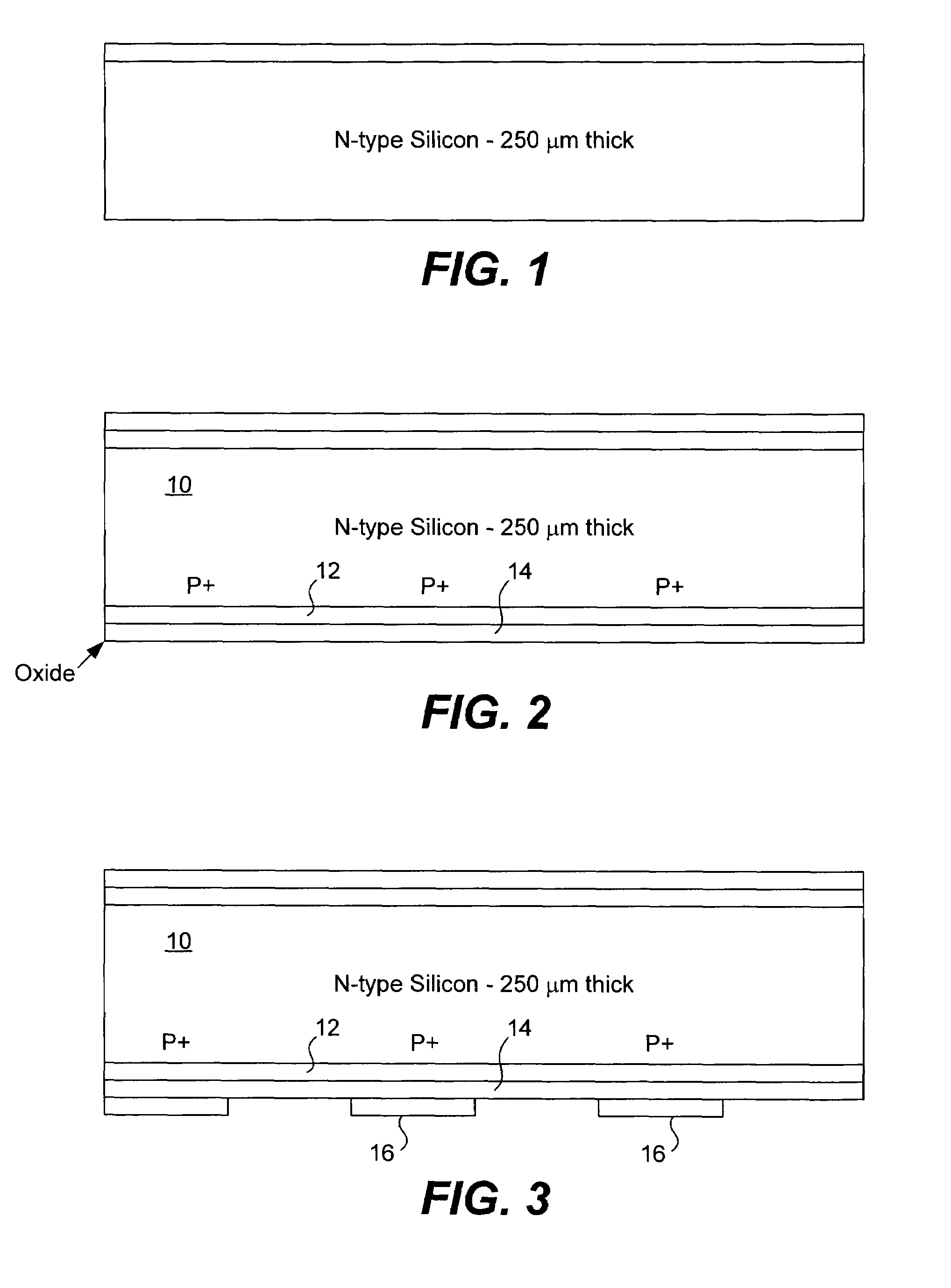
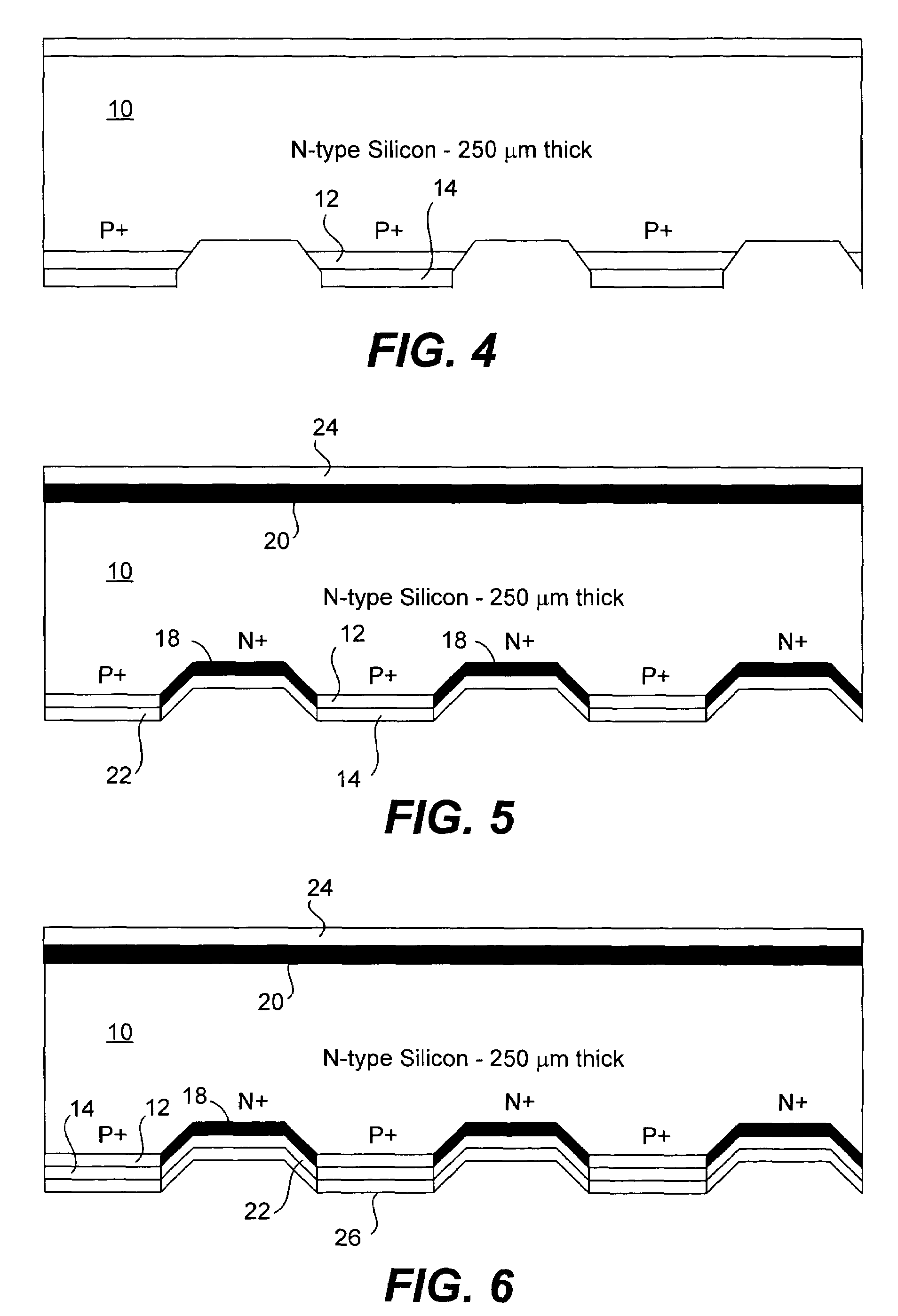
[0013]A solar cell in accordance with the invention is preferably manufactured in a single crystalline silicon substrate having a (100) crystalline orientation or in a multi-crystalline silicon substrate with minority carrier lifetime greater than 200 microseconds. FIG. 1 is a side view in section of such a wafer 10 which is doped n-type in the resistivity range of 1-20 ohm / cm and with a thickness of approximately 200 μm. The first step of the process is caustic etching of the wafer using KOH or NaOH to remove solid damage from ingot wafering. Typically, 20-50 μm of silicon are removed. After the caustic etch, the wafers are cleaned using a standard pre-diffusion, wet cleaning sequence.

[0014]Next, as shown in FIG. 2, the wafer is blanket-diffused on both sides in diffusion boats in a high temperature diffusion furnace. In a preferred embodiment, a liquid boron dopant source (BBr3) is used and a dopant drive forms a p+ layer 12. The dopant drive is followed by growth of a thermal sil...


PUM


Abstract

A solar cell that is readily manufactured using processing techniques which are less expensive than microelectronic circuit processing. In preferred embodiments, printing techniques are utilized in selectively forming masks for use in etching of silicon oxide and diffusing dopants and in forming metal contacts to diffused regions. In a preferred embodiment, p-doped regions and n-doped regions are alternately formed in a surface of the wafer in offset levels through use of masking and etching techniques. Metal contacts are made to the p-regions and n-regions by first forming a seed layer stack that comprises a first layer such as aluminum that contacts silicon and functions as an infrared reflector, second layer such titanium tungsten that acts as diffusion barrier, and a third layer functions as a plating base. A thick conductive layer such as copper is then plated over the seed layer, and the seed layer between plated lines is removed. A front surface of the wafer is preferably textured by etching or mechanical abrasion with an antireflection layer provided over the textured surface. A field layer can be provided in the textured surface with the combined effect being a very low surface recombination velocity.

Description

BACKGROUND OF THE INVENTION[0001]This invention relates generally to solar cells, and more particularly the invention relates to a solar cell structure which is efficient in operation and economical to manufacture.[0002]The use of photovoltaic cells for the direct conversion of solar radiation into electrical energy is well known, see Swanson, U.S. Pat. No. 4,234,352 for example. Briefly, the photovoltaic cell comprises a substrate of semiconductive material having a p-n junction defined therein. In the conventional silicon cell the p-n junction is formed near a surface of the substrate which receives impinging radiation. Radiated photons create mobile carriers (holes and electrons) and the substrate which can be directed to an electrical circuit outside of the cell. Only photons having at least a minimum energy level (e.g., 1.1 electron volt for silicon) can generate an electron-hole pair in the semiconductor pair. Photons having less energy are either not absorbed or are absorbed ...

Claims


Application Information

Patent Timeline
IPC IPC(8): H01L31/00
CPCH01L31/022441H01L31/0682H01L31/1804Y02E10/547Y02P70/50
Inventor MULLIGAN, WILLIAM P.CUDZINOVIC, MICHAEL J.PASS, THOMASSMITH, DAVIDKAMINAR, NEILMCINTOSH, KEITHSWANSON, RICHARD M.
Owner MAXEON SOLAR PTE LTD
Why Eureka
Try Eureka