
Multilayered resist systems using tuned polymer films as underlayers and methods of fabrication thereof

Inactive Publication Date: 2008-04-22
GLOBALFOUNDRIES INC
View PDF10 Cites 22 Cited by
  • Summary
  • Abstract
  • Description
  • Claims
  • Application Information

AI Technical Summary

Benefits of technology

[0014]It is an object of the present invention to provide an improved resist structure.
[0037]Another more specific aspect of the present invention is a multilayer resist system in which the optical, chemical, and physical properties of the underlayer are controlled to prevent interfacial mixing with the resist, interfacial reaction, and diffusion of components from one layer into another.

Problems solved by technology

The need to remain cost and performance competitive in the production of semiconductor devices has driven the industry to a continuing increase in device density with a concomitant decrease in device geometry.
As the thickness of the resist is decreased, the resist becomes less effective as a mask for subsequent dry etch image transfer to the underlying substrate.
Without significant improvement in the etch selectivity exhibited by current single layer resists, these systems can not provide the necessary lithography and etch properties for high resolution lithography.
Another problem with single layer resist systems is critical dimension (CD) control.
Substrate reflections at ultraviolet (UV) and deep ultraviolet (DUV) wavelengths are notorious to produce standing wave effects and resist notching which severely limit CD control of single layer resists.
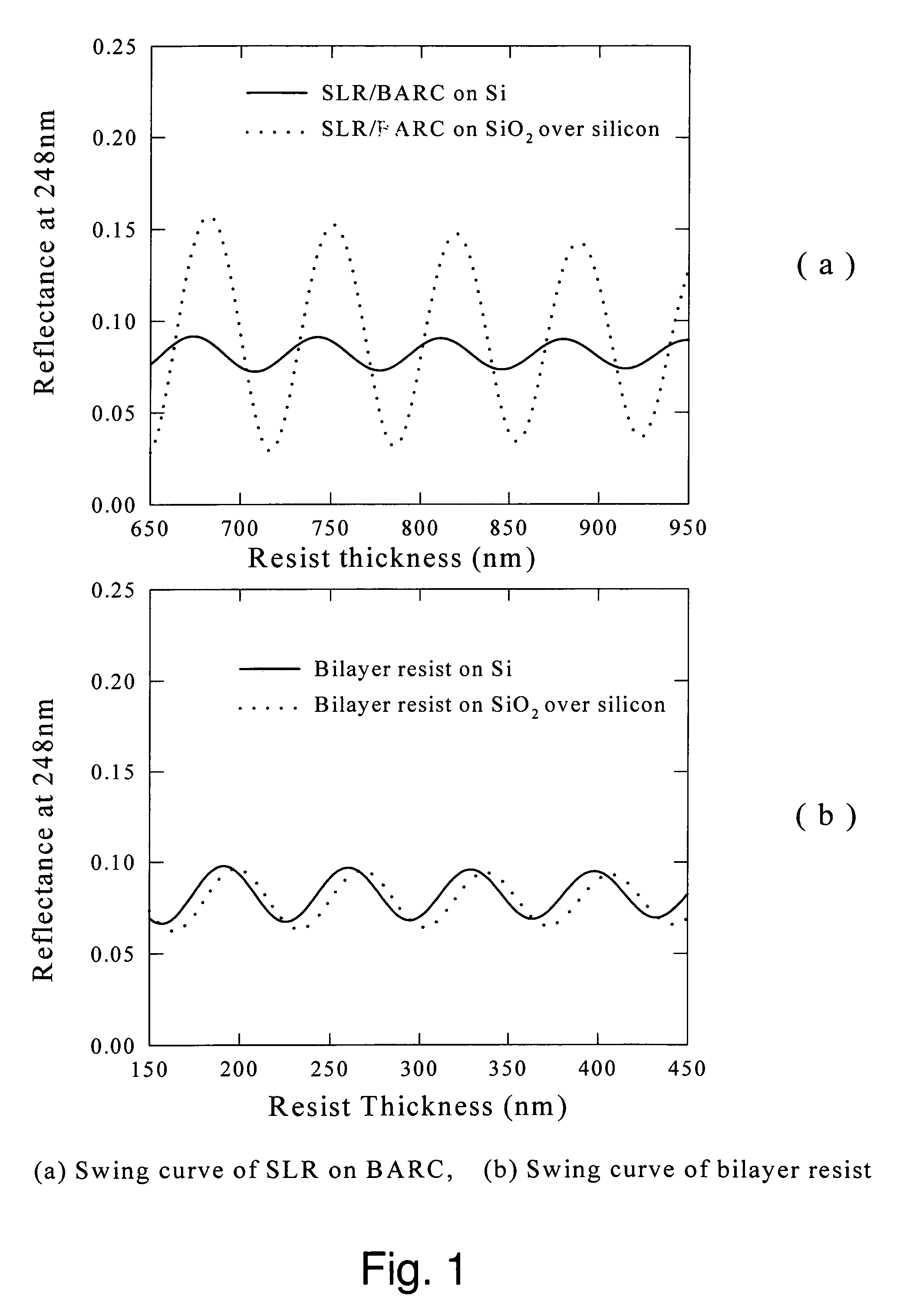
Thin film interference plays a dominant role in CD control of single layer photoresist processes, causing large changes in the effective exposure dose due to a tiny change in optical phase.
However, these thin absorbing BARCs have fundamental limitations.
The thickness of the BARC and the resist can not be controlled to the accuracy required to operate at the target thickness to achieve minimum reflectance.
The thin BARC will generally not effectively planarize this thin underlying films.
When the resist is thin, the microchannels extend into the underlying films creating defects.
It is found that using a typical novolac based underlayer results in an interfacial reaction with the imaging resist, resulting in significant residue and limiting the ultimate resolution.

Method used


Image

  • Multilayered resist systems using tuned polymer films as underlayers and methods of fabrication thereof
  • Multilayered resist systems using tuned polymer films as underlayers and methods of fabrication thereof
  • Multilayered resist systems using tuned polymer films as underlayers and methods of fabrication thereof

Examples


example 1

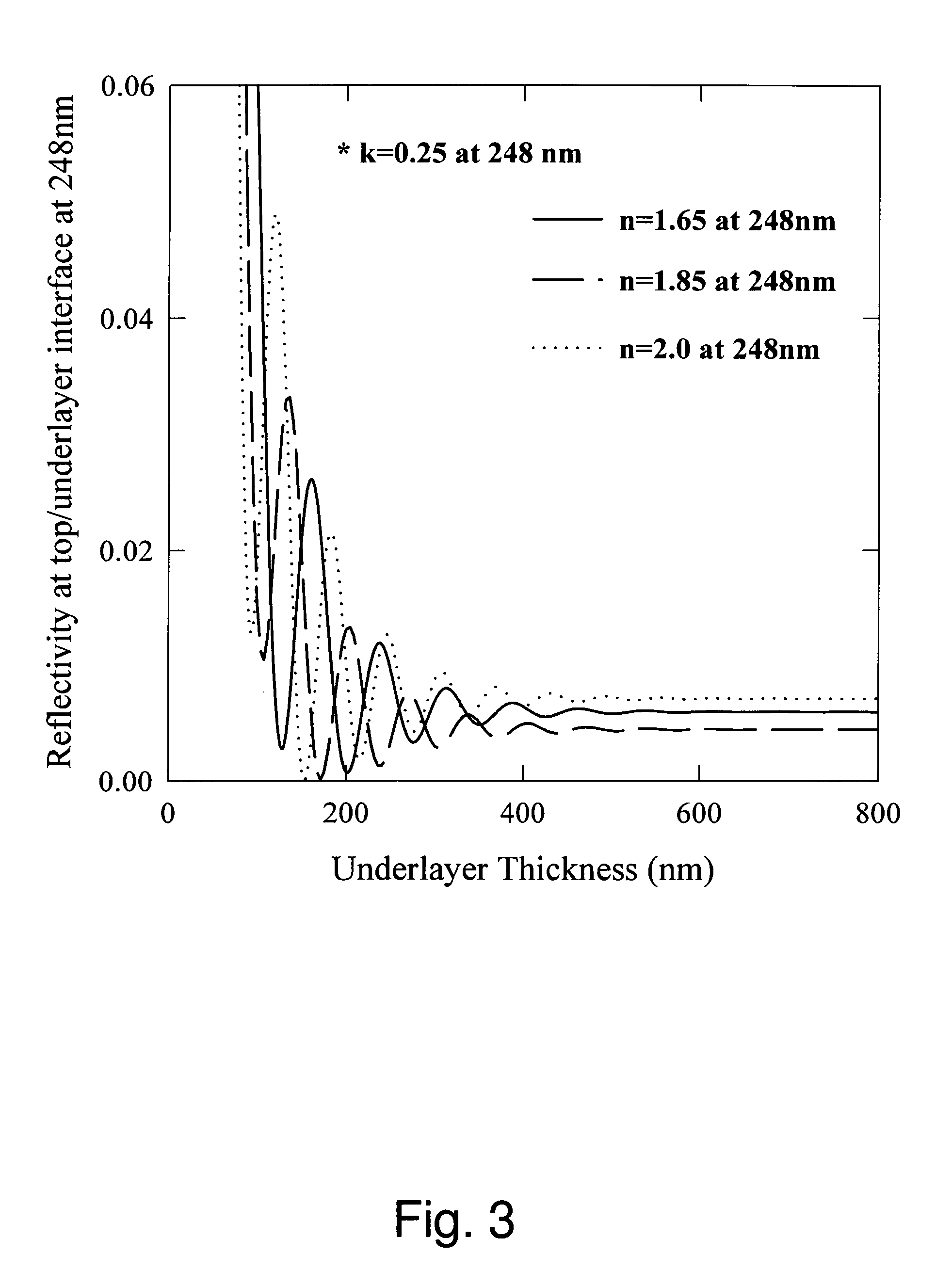
[0082]The following example illustrates calculations for obtaining optimum bottom layer parameters of a bilayer system. Parameters are optimized so as to reduce reflections at the resist / underlayer interface. Computations are based on algorithms which use the Fresnel coefficients as found in standard textbooks such as Optics, by E. Hecht and A. Zajac, published in 1979 by Wiley, pages 312 and 313. These simulations can be extended to many different structures and they are not limited by the examples given below. The structure simulated in this example includes a Si substrate, underlayer and photoresist. The parameters under investigation are the bottom layer optical constants n and k and film thickness d. The imaging Si-containing resist index of refraction extinction coefficient k and film thickness are fixed and given by n=1.78, k=0.018 and d=2000 A at 248 nm. FIG. 3 shows reflectivity at the underlayer / resist interface at 248 nm as a function of underlayer thickness for different...

example 2

[0084]The following example illustrates how to measure the optical constants n and k of the underlayer materials. This measurement technique can be applied to a variety of different processes and it is not limited by the two example above.

[0085]The optical constants were measured using an n&k Analyzer manufactured by n&k Technology, S. Clara, Calif. A description of this instrument and its operation can be found in U.S. Pat. No. 4,905,170, 1990. They use a method based on broadband spectrophotometry and equations for optical constants derived by Forouhi and Bloomer (Phys. Rev. B, 38, pp. 1865-1874, 1988). Their analysis is based on a physical model for the refractive index, n, and extinction coefficient, k, applicable to a wide range of semiconductor and dielectric films, and valid over the deep ultraviolet—near infrared wavelength range. The n(λ) and k(λ) (λ is the wavelength) spectra of any material cannot be measured directly but they are determined from a de-convolution of a ref...

example 3

[0088]The following example is given to demonstrate the tuning of optical properties of novolac / diazonapthoquinone underlayers. The optical properties of the coated novolac / diazonapthoquinone materials that described in this example are: 1) the index of refraction (n) at 248 nm, 2) the extinction coefficient (k) at 248 nm and 3) the absorption coefficient (α) 248 nm was calculated from equation (1) above. Shipley grade 2 novolak had been spun coated onto 8″ wafers then soft baked at 120C for 30 seconds and hard baked at four different temperatures: 225, 250, 252, 275 and 300 degrees C. for 90 seconds using contact hotplates. Optical properties of novolac films measured by method described in example 2 and summarized in Table 1. We have found a strong correlation between the optical properties of novolak underlayers and processing conditions. Novolac underlayers found hard to control due to high dependance of n and k values on process temperature.


PUM


Abstract

Disclosed are multilayered resist structures including bilayer and top surface imaging which utilize tuned underlayers functioning as ARCs, planarizing layers, and etch resistant hard masks whose properties such as optical, chemical and physical properties are tailored to give a multilayer resist structure exhibiting high resolution, residue free lithography and methods of preparing these materials. These underlayer films include the group consisting of novolac based resists whose processing conditions are controlled, polyarylsulfones such as the BARL material, polyhydroxystyrene based derivatives, an example being a copolymer of polyhydroxystyrene and polyhydroxystyrene reacted with anthracenemethanol that contains a cross-linker, and acid catalyst (thermal acid generator), polyimides, polyethers in particular polyarylene ethers, polyarylenesulfides, polycarbonates such as polyarylenecarbonates, epoxies, epoxyacrylates, polyarylenes such as polyphenylenes, polyarylenevinylenes such as polyphenylenevinylenes, polyvinylcarbazole, cyclicolefins, and polyesters. Such films have index of refraction and extinction coefficient tunable from about 1.4 to about 2.1 and from about 0.1 to about 0.6 at UV and DUV wavelengths, in particular 365, 248, 193 and 157 nm and EUV. Moreover, underlayer films produced in the present invention do not interact with the resist limiting interfacial mixing and contamination of resist by an outgassing product. The bilayer and TSI resist structures can be used for 248, 193, 157, EUV, x-ray, e-beam, and ion beam technology.

Description

[0001]This application claims priority from Provisional Application Ser. No. 60 / 075,567 which was filed on Feb. 23, 1998.FIELD OF THE INVENTION[0002]The present invention is directed to structures useful for fabricating integrated circuits (IC), in particular structures having a plurality of layers. More particularly, the present invention is directed to multilayer resist structures having underlayers whose properties such as optical, chemical and physical properties are tailored to give a multilayer resist structure exhibiting high performance and high resolution. Such a multilayer resist structure can be used for optical, electron beam, x-ray, ion beam, and euv lithography.BACKGROUND OF THE INVENTION[0003]The need to remain cost and performance competitive in the production of semiconductor devices has driven the industry to a continuing increase in device density with a concomitant decrease in device geometry. To facilitate the shrinking device dimensions, new lithographic materi...

Claims


Application Information

Patent Timeline
IPC IPC(8): G03F7/023
CPCG03F7/091Y10S430/145
Inventor ANGELOPOULOS, MARIEBABICH, KATHERINA E.LATULIPE, DOUGLAS CHARLESLIN, QINGHUANGMEDEIROS, DAVID R.MOREAU, WAYNE MARTINPETRILLO, KAREN E.SIMONS, JOHN P.
Owner GLOBALFOUNDRIES INC
Learn More