

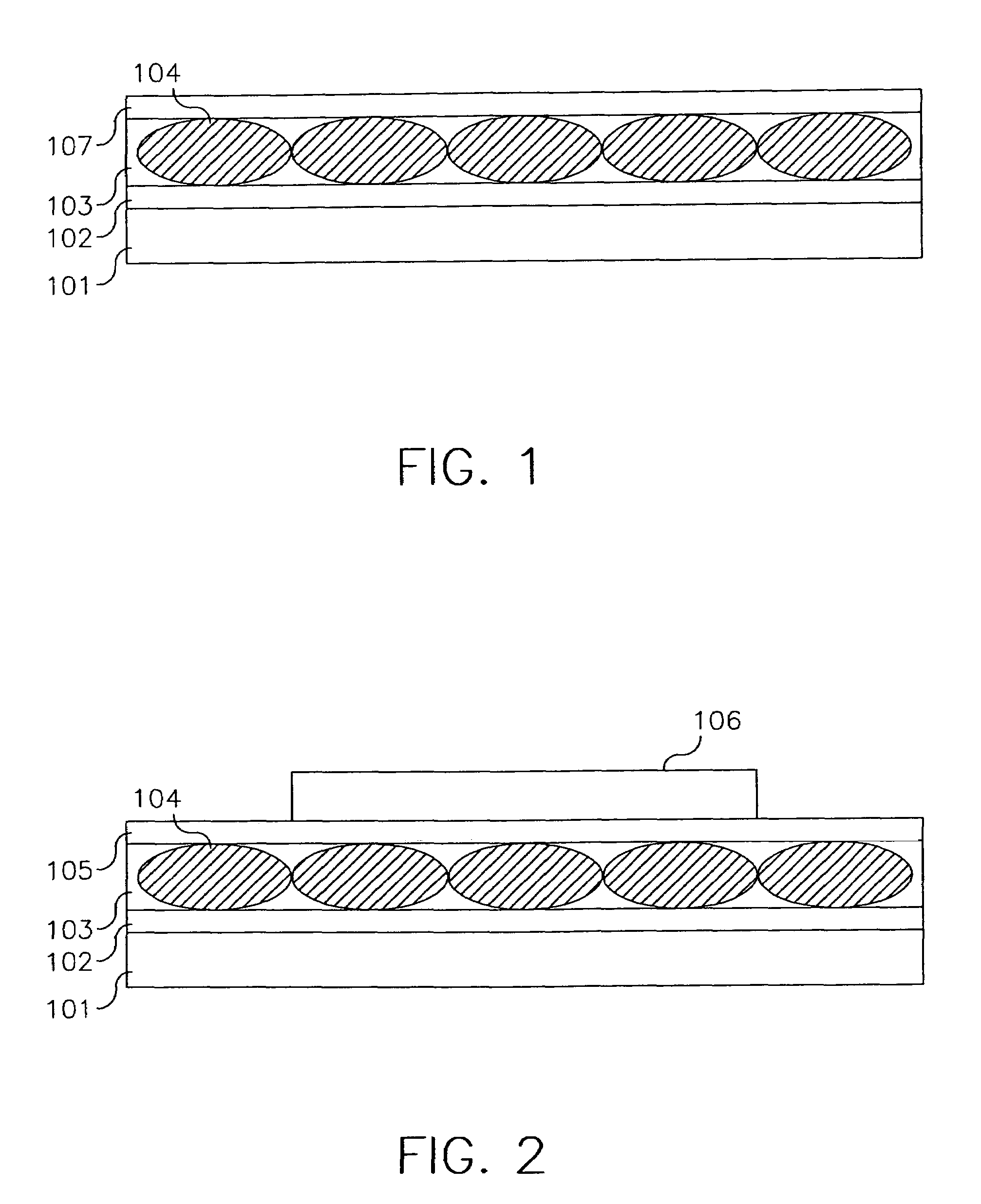
Display comprising liquid crystal droplets in a hydrophobic binder
a technology of hydrophobic binders and liquid crystal droplets, which is applied in the direction of thin material processing, material nanotechnology, instruments, etc., can solve the problems of loss of performance, change in reflected color, ultraviolet radiation harmful to liquid crystals, etc., and achieve low switching voltage, high contrast, and low cost
- Summary
- Abstract
- Description
- Claims
- Application Information
AI Technical Summary
Benefits of technology
Problems solved by technology
Method used
Image

Examples
example 1 (
INVENTION)
[0120]A chiral nematic composition with center wavelength of reflection (CWR) of 590 nm was prepared by adding the appropriate amount of a high twist chiral dopant to the nematic host mixture BL087 obtained from Merck, Darmstadt, Germany.
[0121]A dispersion of the cholesteric liquid crystal composition with CWR at 590 nm was prepared as follows. To 502 grams of distilled water was added 7.5 grams of Ludox TM colloidal silica suspension and 15.5 grams of a 10% w / w aqueous solution of a copolymer of methylaminoethanol and adipic acid. To this was added 225 grams of the cholesteric liquid crystal composition. The mixture was stirred using a Silverson mixer at 5000 rpm. It was then passed through a microfluidizer at 3000 psi. Finally, the resulting dispersion was passed through a 23 μm filter. The droplet size distribution in the dispersion was measured using a Coulter Counter. It was found that the mean size was 9.5 microns and the coefficient of variation (cv) was 0.14.
[0122]...
example 2 (
CONTROL)
[0125]A chiral nematic composition with center wavelength of reflection (CWR) of 590 nm was prepared by adding the appropriate amount of a high twist chiral dopant to the nematic host mixture BL087 obtained from Merck, Darmstadt, Germany.
[0126]A dispersion of the cholesteric liquid crystal composition with CWR at 590 nm was prepared as follows. To 502 grams of distilled water was added 7.5 grams of Ludox TM colloidal silica suspension and 15.5 grams of a 10% w / w aqueous solution of a copolymer of methylaminoethanol and adipic acid. To this was added 225 grams of the cholesteric liquid crystal composition. The mixture was stirred using a Silverson mixer at 5000 rpm. It was then passed through a microfluidizer at 3000 psi. Finally, the resulting dispersion was passed through a 23 μm filter. The droplet size distribution in the dispersion was measured using a Coulter Counter. It was found that the mean size was 9.5 microns and the coefficient of variation (cv) was 0.14.
[0127]Th...
example 3 (
CONTROL)
[0130]Example 3 demonstrates the results achieved when coating or printing a conductive layer onto a liquid crystal layer, with a barrier layer, resulting in increased thickness, to protect the liquid crystal layer from the carrier solvent for the conductive layer.
[0131]A chiral nematic composition with center wavelength of reflection (CWR) of 590 nm was prepared by adding the appropriate amount of a high twist chiral dopant to the nematic host mixture BL087 obtained from Merck, Darmstadt, Germany.
[0132]A dispersion of the cholesteric liquid crystal composition with CWR at 590 nm was prepared as follows. To 502 grams of distilled water was added 7.5 grams of Ludox TM colloidal silica suspension and 15.5 grams of a 10% w / w aqueous solution of a copolymer of methylaminoethanol and adipic acid. To this was added 225 grams of the cholesteric liquid crystal composition. The mixture was stirred using a Silverson mixer at 5000 rpm. It was then passed through a microfluidizer at 300...
PUM
| Property | Measurement | Unit |
|---|---|---|
| thickness | aaaaa | aaaaa |
| surface roughness | aaaaa | aaaaa |
| thickness | aaaaa | aaaaa |
Abstract
Description
Claims
Application Information