Method and apparatus for inspecting integrated circuit pattern

a technology of integrated circuit and pattern inspection, which is applied in the direction of individual semiconductor device testing, instruments, nuclear engineering, etc., can solve the problems of failure to detect etching remainder or incomplete-open failure in micro conductor holes smaller than the resolution of optical systems, failure to detect defects generated in wiring-pattern stepped bottom portions, and high efficiency. , the effect of high yield

Inactive Publication Date: 2008-08-26
HITACHI LTD
View PDF46 Cites 24 Cited by
  • Summary
  • Abstract
  • Description
  • Claims
  • Application Information

AI Technical Summary

Benefits of technology

[0019]A second object of the present invention is to acquire an electron-beam image as a good-quality image which is high in the speed, good in the stability, high in the resolution, high in the contrast and large in the SN ratio in order to perform inspection by using the aforementioned electron-beam image so that a defect generated on a micro circuit pattern can be detected accurately in comparison and inspection.
[0038]producing process by using this method and apparatus, a failure or defect which is generated in the shape of the pattern by a process and which could not be detected in a semiconductor device in every step by the conventional technique, can be detected in an early stage. As a result, problems which are latent in processes, production apparatus conditions, and so on, can be actualized. Accordingly, a countermeasure against the cause of failure in high-speed high-accurate processes of producing various kinds of substrates such as semiconductor devices compared with the conventional processes can be taken. Accordingly, not only a high yield, that is, a high efficiency percentage can be secured but also high accurate inspection can be made because error detection which occurs in inspection and becomes a problem is reduced.

Problems solved by technology

If a semiconductor wafer in a way of producing process was inspected by such an optical inspection method, the pattern residue or defect having a light-transmissible silicon oxide film or a photoresist material on its surface could not be detected.
Further, an etching remainder or a incomplete-open failure in a micro conduct hole smaller than the resolution of an optical system could not be detected.
Further, a defect generated in a wiring-pattern stepped bottom portion could not be detected.
As described above, with the advance of reduction in size of the circuit pattern and complication in shape of the circuit pattern and with the advance of diversification of the material, it has become difficult to detect a defect by using an optical image.
Further, in a large-current and low-accelerated electron beam, it is difficult to acquire a high-resolution image because of a space-charge effect.
A detecting apparatus of this type is, however, poor in frequency responsibility because light emission from the fluorescent material is detected, so that the detecting apparatus of this type is unsuitable for formation of an electron beam image at a high speed.
When a circuit pattern in a process for producing a micro-structure semiconductor device was detected by using the aforementioned prior art optical inspection method, it was possible to detect the residue of a silicon oxide film, a resist material, or the like, which was formed from an optically transmissible material and which was sufficiently short in the optical distance depending on the optical wavelength and refractive index used for inspection, and it was difficult to detect an etching remainder or a incomplete-open failure in a micro conduct hole which was linear so that the width of a short side thereof was not larger than the resolution of an optical system.
On the other hand, in the observation and inspection using the SEM, there are two problems as follows.
One problem is that a very long time is required for inspecting a circuit pattern on the whole surface of a semiconductor wafer because the conventional method, by means of the SEM, for forming an electron-beam image needs a very long time.
The other problem was that it was difficult to obtain a stable contrast image in inspection by means of an electron beam and to obtain a predetermined value of inspection accuracy in the case where the material constituting a circuit pattern as a subject to be inspected was formed from an electrically insulating material such as a resist, a silicon oxide film, or the like, or in the case where the material was formed from a mixture of an electrically insulating material and an electrically conducting material.
In this conventional technique, however, there is no description about a method for adjusting the inspection condition with respect to a material such as an electrically insulating material, or the like.
Accordingly, this conventional technique is unsuitable for inspecting a wide region at a high speed because a long time is required for acquiring the electron-beam image.
Further, even in the case where charge in the local region is stable, it is difficult that another region to be compared is controlled to be in the same charge state.
For example, it is difficult to inspect a wide region of a semiconductor wafer, or the like.
Because the state of charge changes with the passage of time correspondingly to the irradiation time as described above, the image signal changes during integration so that it is difficult to obtain stable contrast.
As described in the prior art, with a large-current and low-accelerated electron beam, it is difficult to obtain an image of high resolution because of the space-charge effect.
Because an electric field generated by the negative voltage for deceleration acts on the secondary electrons to accelerate the secondary electrons to energy of the order of kV, it is difficult to collect the high-speed secondary electrons to a detector.
If the quantity of deflection is selected to be too large, there arises a problem that the secondary electrons collide with a deflection plate per se of the ExB deflector so that the secondary electrons cannot be led to the detector.
Further, if the deflection by the ExB deflector is selected to be intensive, there arises a problem that aberration occurs in the primary electron beam so that it is difficult to converge the electron beam on a surface of the sample substrate through an objective lens, or the like.
Accordingly, there arises a problem that noise generated from the light-emitting element and the light-receiving element is added to the original analog signal to lower the SN ratio in the secondary electron signal.

Method used


Image

  • Method and apparatus for inspecting integrated circuit pattern
  • Method and apparatus for inspecting integrated circuit pattern
  • Method and apparatus for inspecting integrated circuit pattern

Examples


embodiment 1

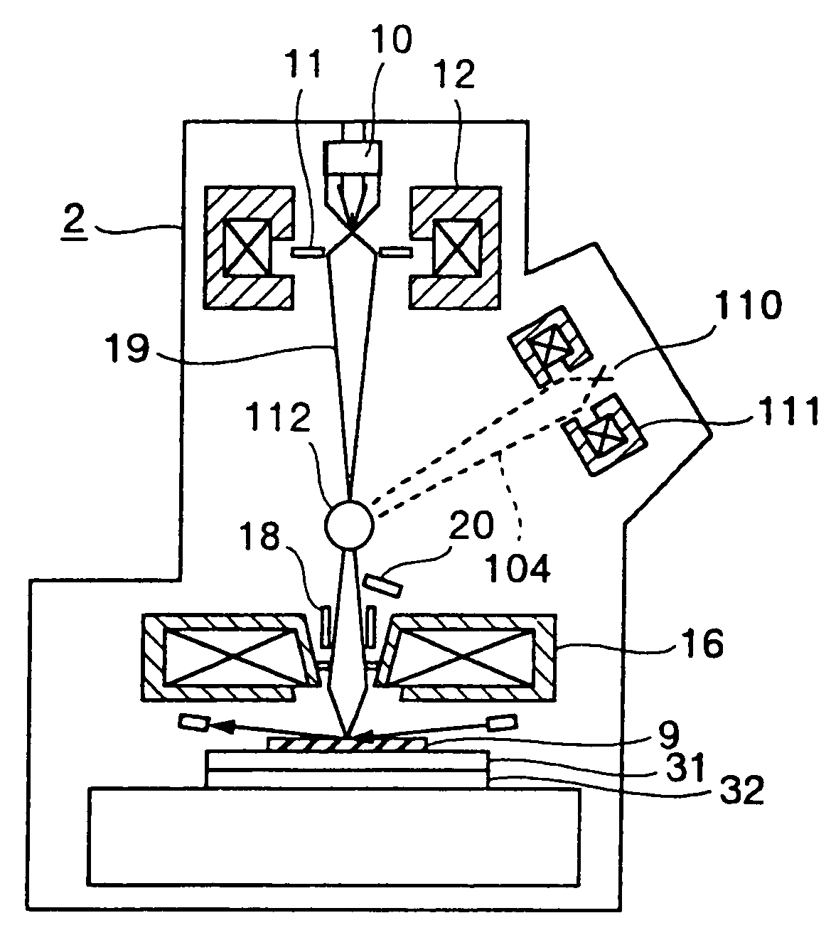
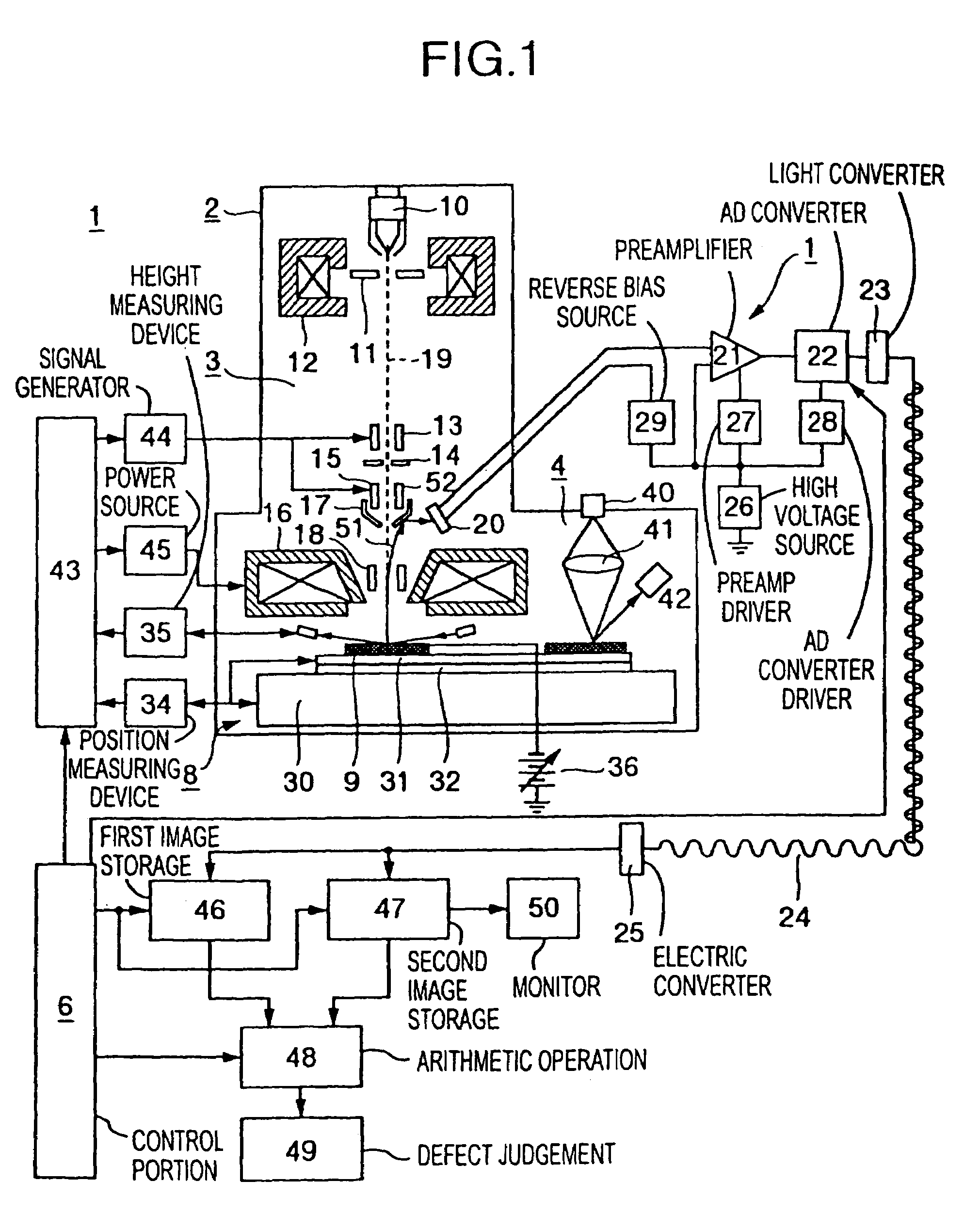
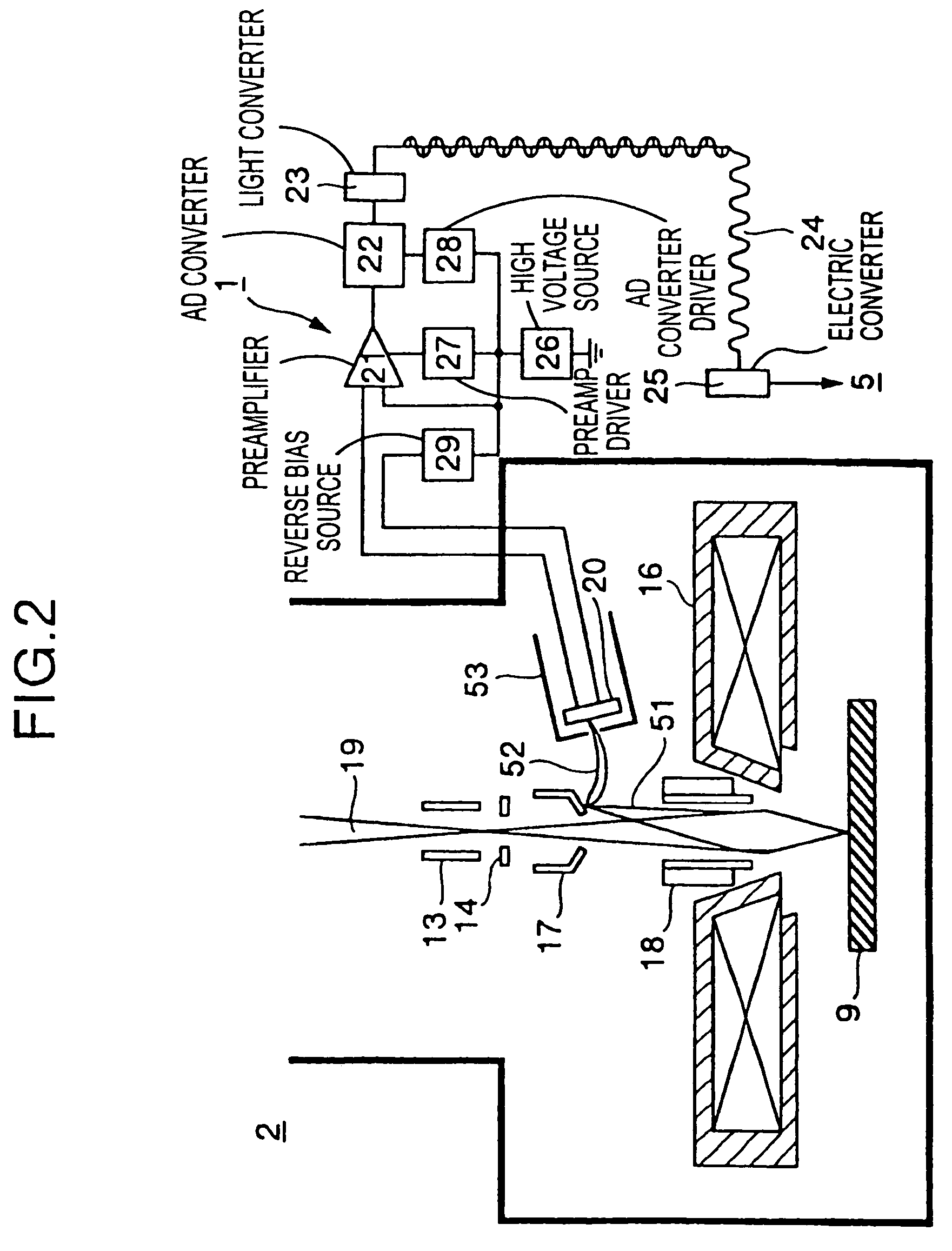
[0057]FIG. 1 shows the configuration of a circuit pattern inspection apparatus 1 according to a first embodiment of the present invention. The circuit pattern inspection apparatus 1 has an inspection chamber 2 to be evacuated, and a sub chamber (not shown in this embodiment) for carrying a sample substrate 9 into the inspection chamber 2. The sub chamber is configured so as to be able to be evacuated independently of the inspection chamber 2. The circuit pattern inspection apparatus 1 is constituted by a control portion 6, an image processing portion 5 in addition to the inspection chamber 2 and the sub chamber. The inside of the inspection chamber 2 is roughly constituted by an electronic optical system 3, a secondary electron detection portion 7, a sample chamber 8, and an optical microscope portion 4. The electronic optical system 3 has an electron gun 10, an electron beam extracting electrode 11, a condenser lens 12, a blanking deflector 13, a scanning deflector 15, an aperture ...

embodiment 2

[0089]In this embodiment, there will be described an applied example in which a semiconductor wafer is inspected by using the circuit pattern inspection apparatus 1 and method according to the present invention. FIG. 6 shows a process for producing a semiconductor device. As shown in FIG. 6, a large number of pattern forming processes are repeated in the semiconductor device. The pattern forming process is roughly constituted by the steps of deposition, application of a light-sensitive resist, exposure, development, etching, resist removal and cleaning. If the production condition for processing is not optimized in each step, a circuit pattern of the semiconductor device formed on the substrate is not formed normally. FIGS. 7(a) and 7(b) schematically show a circuit pattern formed on a semiconductor wafer in a production process. FIG. 7(a) shows a circuit pattern processed normally, and FIG. 7(b) shows a circuit pattern in which a failure in processing occurs. When, for example, abn...

embodiment 3

[0092]The third embodiment of the present invention as to the configuration of the inspection apparatus is configured in the same manner as in the first embodiment except that an objective lens 16 in the electronic optical system 3 is disposed above the secondary electron detector 20 as shown in FIG. 8. FIG. 8 shows an enlarged partial view of the inside of the inspection chamber 2 in the circuit pattern inspection apparatus. The operation based on the configuration of the third embodiment will be described below. An electron beam 19 is irradiated onto an inspection-subject substrate 9 in the same method as in the first embodiment. A negative high voltage is applied to the inspection-subject substrate 9 in the same manner as in the first embodiment. In this embodiment, the negative voltage for retarding primary electrons applied to the inspection-subject substrate 9 is selected to be −3.5 keV. By electron beam irradiation, secondary electrons 51 are generated from a surface of the s...


PUM


Abstract

A circuit pattern inspection method and an apparatus therefor, in which the whole of a portion to be inspected of a sample to be inspected is made to be in a predetermined charged state, the portion to be inspected is irradiated with an image-forming high-density electron beam while scanning the electron beam, secondary charged particles are detected at a portion irradiated with the electron beam after a predetermined period of time from an instance when the electron beam is irradiated, an image is formed on the basis of the thus detected secondary charged particle signal, and the portion to be inspected is inspected by using the thus formed image.

Description

[0001]This is a continuation application of U.S. Ser. No. 10 / 379,555, filed Mar. 6, 2003 now U.S. Pat. No. 7,026,830; which is a continuation application of U.S. Ser. No. 09 / 983,703, filed Oct. 25, 2001, now U.S. Pat. No. 6,559,663; which is a continuation application of U.S. Ser. No. 09 / 525,341, filed Mar. 14, 2000, now U.S. Pat. No. 6,329,826; which is a continuation application of U.S. Ser. No. 08 / 811,511, filed Mar. 4, 1997, now U.S. Pat. No. 6,172,363.BACKGROUND OF THE INVENTION[0002]The present invention relates to a method and apparatus for producing a substrate having a micro circuit pattern for a semiconductor device, a liquid crystal, or the like, and particularly relates to a technique for inspecting a pattern for a semiconductor device or a photomask, that is, the present invention relates to a technique for inspecting a pattern on a wafer in a way of semiconductor device producing process and a technique for performing comparison and inspection by using an electron beam...

Claims


Application Information

Patent Timeline
Patent Type & Authority Patents(United States)
IPC IPC(8): G01R31/305H01J37/28G01Q30/02G01Q30/04G01R31/307
CPCG01R31/305H01J37/28G01R31/307H01J2237/2817
Inventor SHINADA, HIROYUKINOZOE, MARIYODA, HARUOANDO, KIMIAKIKURODA, KATSUHIROKANEKO, YUTAKATANAKA, MAKIMAEDA, SHUNJIKUBOTA, HITOSHISUGIMOTO, ARITOSHISUGIYAMA, KATSUYATAKAFUJI, ATSUKOYAJIMA, YUSUKETOOYAMA, HIROSHIINO, TADAOHIROI, TAKASHIYOSHIMURA, KAZUSHIUSAMI, YASUTSUGU
Owner HITACHI LTD
Why Eureka
Try Eureka