Formation of metal oxide nanowire networks (nanowebs) of low-melting metals

a technology of nanowires and metal oxides, applied in the direction of polycrystalline material growth, crystal growth process, condensed vapor, etc., can solve the problems of web-like structures, amorphous, slow tools, and cost-prohibitive for the assembly of large-area networks of nanomaterials

Inactive Publication Date: 2008-11-04
UNIV OF LOUISVILLE +2
View PDF3 Cites 18 Cited by
  • Summary
  • Abstract
  • Description
  • Claims
  • Application Information

AI Technical Summary

Benefits of technology

[0011]Two-dimensional networks of nanowires and nanotubes of β-Ga2O3 were obtained using hydrogen / oxygen plasma exposure of gallium droplets covered substrate. Multiple nucleation and growth of one dimensional structures from the gallium droplets parallel to the substrate coalesced to yield the crystalline network. Because of the unique regular arrangement of nanowires in a polygonal fashion, these crystalline networks are described as ‘nanowebs’. The molecular arrangement of the Ga2O3 nanowires / nanotubules suggests that key electrical properties be associated with these structures. The formation mechanism and evolution of Ga2O3 nanowebs suggests that this process could be easily extended to other low melting metal oxides such as SnO2, ZnO and In2O3 etc.
[0013]Low melting metals (for example, gallium) provide the solvent medium for bulk nucleation and growth of nanowires, thereby eliminating the need for transition metal clusters as growth templates. Large droplets (millimeter size) or thin gallium films are spread on substrates to initiate nucleation with densities greater than 1011 / cm2. The large number density of the resulting nanowires makes the technique suitable and interesting for large-scale production. The gas phase chemistry can be used to manipulate the absolute size, composition, and crystallinity of the nanowires. The only requirement is that the materials of interest should have extremely low solubility and low wetting characteristics with respect to molten gallium. If the solute wets the molten metal then two-dimensional crystals (platelets) or three-dimensional crystals are more likely to result rather than one-dimensional crystals.
[0015]The present invention provides a method for the synthesis of oxide nanowebs of low-melting metals with a specific example of a highly crystalline b-gallium oxide nanowire network using molten gallium and a microwave plasma based gas chemistry. Gallium oxide nanowires, 20-100 nm thick and tens to hundreds of microns long were synthesized and confirmed to be crystalline and devoid of any structural defects using transmission electron microscopy. Multiple nucleation and growth of gallium oxide nanowires were obtained with appropriate gas phase composition of hydrogen and oxygen. Direct use of gallium melts in plasma environments allowed bulk synthesis with high nucleation densities and also allowed template-free synthesis of nanostructures with unique geometries. This plasma-based technique allowed for synthesis at temperatures much lower than conventional methods. The gas phase chemistry allowed manipulation of the nanostructure composition, structure, and morphology. Demonstration of this technique with gallium oxide presents a new route for synthesis of nanostructures of other important metal oxides such as indium oxide, tin oxide, and zinc oxide. Synthesis of unique geometrical structures of crystalline gallium oxide in the form of tubes and nanopaintbrushes has been developed.
[0016]Results show that multiple nucleation and growth of gallium oxide nanostructures occur directly out of molten gallium upon exposure to appropriate composition of hydrogen and oxygen in the gas phase. It is possible to present a growth model for the observed morphologies in the one-dimensional structures. Oxygen from the vapor phase forms surface adsorbed species on the molten metal surface. These oxygenated species dissolve into the molten metal followed by phase segregation to create multiple nuclei on the surface. In the absence of hydrogen in the plasma, these nuclei aggregate to form a polycrystalline crust on the molten metal surface. However hydrogen / oxygen chemistry enables nuclei segregation on the metal surface, preventing the complete crust formation. These nuclei grow in one dimension upon basal attachment of the bulk growth species. The surface dynamics of nuclei on the metal surface, i.e., pattern formation, and the time of coalescence determine the morphology of the resulting structure. Thus, results show that the gas phase chemistry allows manipulation of the nanostructure composition, structure, and morphology.
[0023]It is another object of the present invention to provide a method of control over the morphology of the one-dimensional nanostructures due to manipulability of the gas phase chemistry alone.

Problems solved by technology

Although nanoscale metal oxide networks have been fabricated previously, the current techniques produce porous, amorphous, web-like structures.
However, these tools are still too slow and cost-prohibitive for the assembly of large-area networks of nanomaterials for device fabrication.

Method used


Image

  • Formation of metal oxide nanowire networks (nanowebs) of low-melting metals
  • Formation of metal oxide nanowire networks (nanowebs) of low-melting metals
  • Formation of metal oxide nanowire networks (nanowebs) of low-melting metals

Examples


example 1

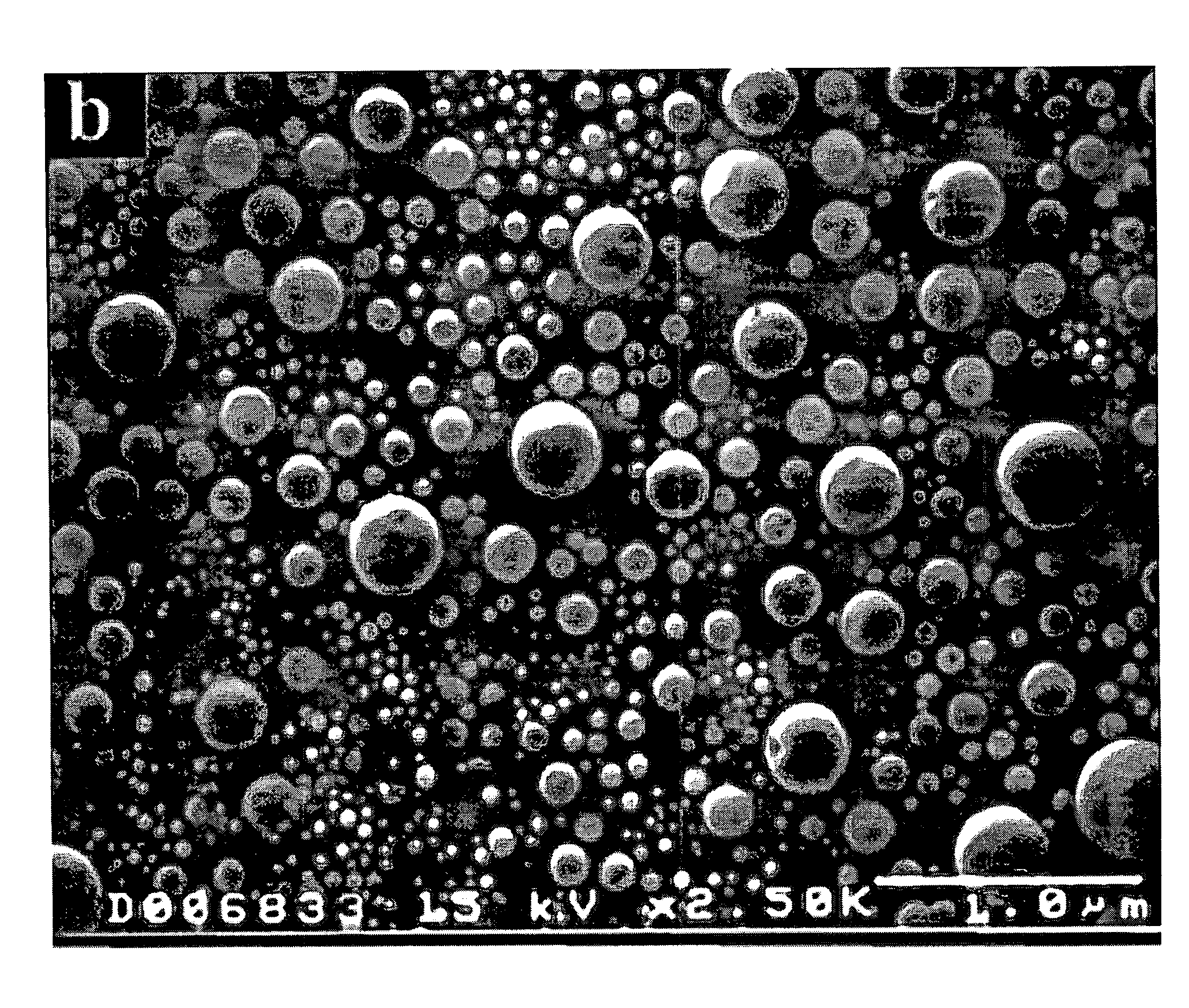
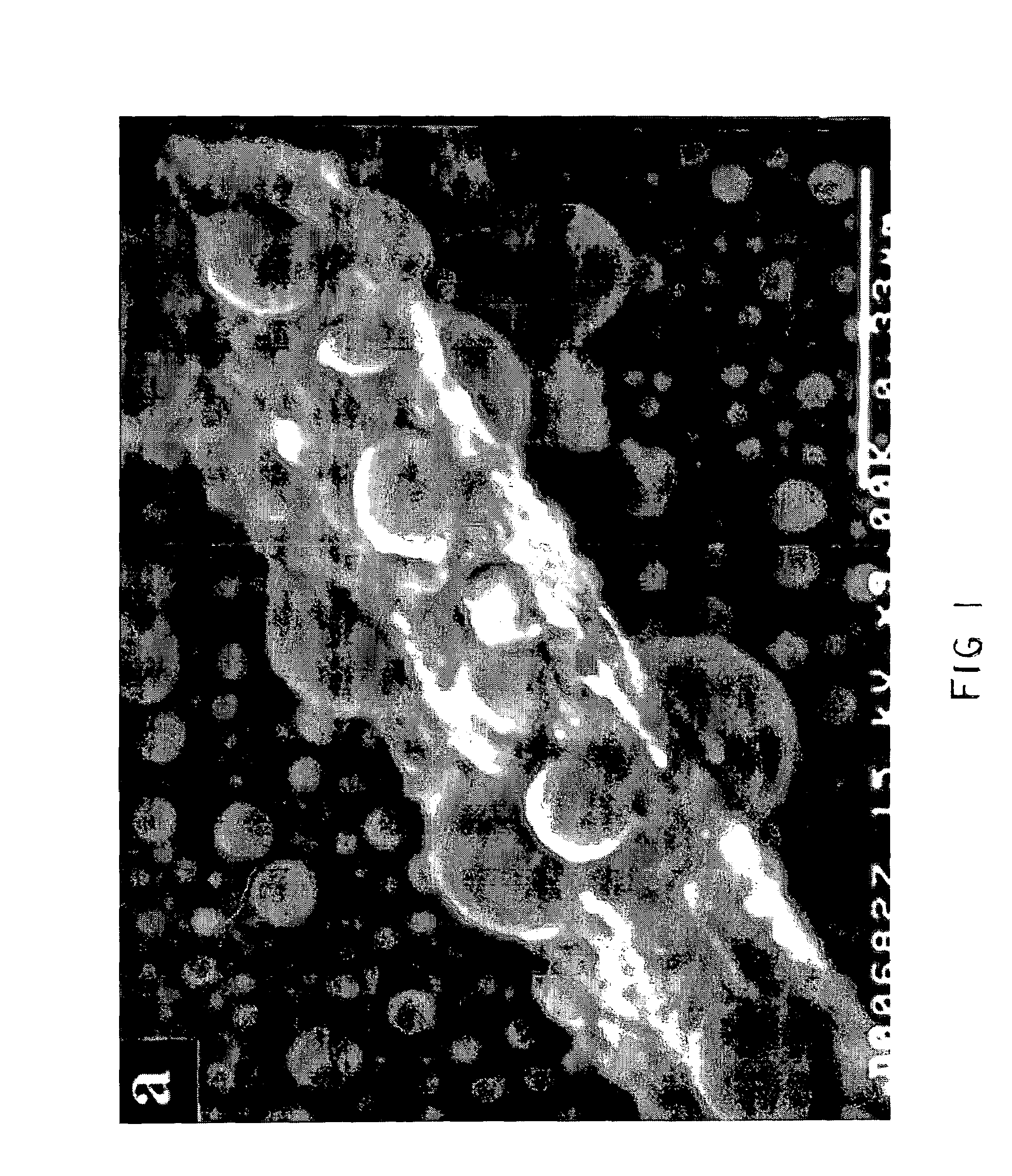
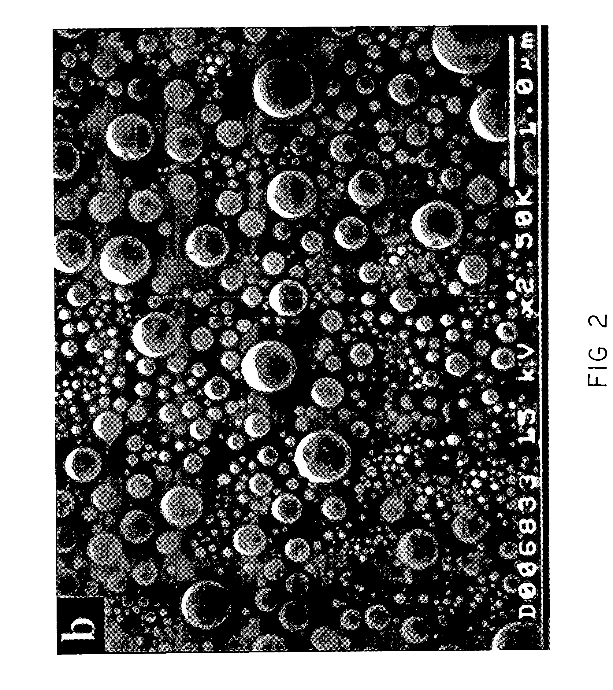
[0090]Commercially available gallium oxide powder (Alfa Aesar) was dispersed in acetone and ultrasonicated for 2 minutes. Five drops of the well-dispersed suspension were then dropped on a 1 cm×1 cm quartz substrate and allowed to dry naturally. The resulting deposit on the substrate constituted a dense packed agglomerate of polycrystalline gallium oxide particles. (SEM showed precursor particles ranged from 50-300 microns). The gallium oxide film was then exposed to hydrogen plasma followed by hydrogen-oxygen plasma. The plasma treatments were done in a microwave plasma reactor (ASTEX 5010) at the following range of process conditions: Microwave power of 500-1200 W, pressure of 20-60 Torr, 2-30 minutes of hydrogen plasma treatment, 15 minutes to 3 hours of plasma treatment to a mixture of hydrogen and oxygen (0.6 20 sccm O2 / 100 sccm in the feed gas). The substrate temperature was measured using an infrared pyrometer to be approximately 550° C. for 700 W microwave power, 40 Torr tot...

example 2

Two-Dimensional Nanostructures: Nanowire Networks (Nanowebs)

[0091]The small clusters (<100 nm) of Ga tend to flatten out with exposure to wetting gas phase species such as nitrogen or oxygen. The nanowires nucleating from these small clusters tend to grow parallel to the substrate and physically impinge on each other. The schematic of FIG. 17 shows nanoweb formation. The studies using oxygen and hydrogen in the gas phase over small clusters of Ga over quartz substrate led to the formation of two-dimensional network of nanowires. The individual segments of the network were on the order of few nm (<10 nm). The entire process is rapid and takes place within few minutes over large areas. The gallium oxide nanoweb is shown as a high-resolution WEM image and high-resolution TEM image as shown in FIGS. 18 and 19, respectively.

[0092]It is contemplated that electrical contacts can be formed to large area nanowire networks and used for sensors (tin oxide and zinc oxide). It is expected that t...


PUM

PropertyMeasurementUnit
lengthaaaaaaaaaa
thickaaaaaaaaaa
lengthaaaaaaaaaa

Abstract

A method of producing networks of low melting metal oxides such as crystalline gallium oxide comprised of one-dimensional nanostructures. Because of the unique arrangement of wires, these crystalline networks defined as “nanowebs”, “nanowire networks”, and / or “two-dimensional nanowires”. Nanowebs contain wire densities on the order of 109 / cm2. A possible mechanism for the fast self-assembly of crystalline metal oxide nanowires involves multiple nucleation and coalescence via oxidation-reduction reactions at the molecular level. The preferential growth of nanowires parallel to the substrate enables them to coalesce into regular polygonal networks. The individual segments of the polygonal network consist of both nanowires and nanotubules of β-gallium oxide. The synthesis of highly crystalline noncatalytic low melting metals such as β-gallium oxide tubes, nanowires, and nanopaintbrushes is accomplished using molten gallium and microwave plasma containing a mixture of monoatomic oxygen and hydrogen. Gallium oxide nanowires were 20-100 nm thick and tens to hundreds of microns long. Transmission electron microscopy (TEM) revealed the nanowires to be highly crystalline and devoid of any structural defects. Results showed that multiple nucleation and growth of gallium oxide nanostructures can occur directly out of molten gallium exposed to appropriate composition of hydrogen and oxygen in the gas phase. The method of producing nanowebs is extendible to other low melting metals and their oxides such as for example: zinc oxide, tin oxide, aluminum oxide, bismuth oxide, and titanium dioxide.

Description

[0001]This is a Continuation in Part application claiming priority from U.S. Pat. No. 7,182,812 issued on Feb. 27, 2007 from application Ser. No. 10 / 664,072 filed on Sep. 16, 2002 and U.S. Pat. No. 7,252, 811 issued on Aug. 7, 2007 from Ser. No. 10 / 187,460 filed on Jul. 1, 2002 and U.S. Pat. No. 6,806,228 issued on Oct. 19, 2004 from Ser. No. 09 / 896,834 filed on Jun. 29, 2000 and provisional application Ser. No. 60 / 478,788 filed on Jun. 16, 2003 and Ser. No. 60 / 478,793 filed on Jun. 16, 2003. all of which are hereby incorporated by reference herein.[0002]This application is part of a government project. The research leading to this invention was supported from the Commonwealth of Kentucky, from a NSF for CAREER grant (CTS 9876251) and U.S. Air Force grant through AFOSR F 49620-00-1-0310. The United States Government retains certain rights in this invention.BACKGROUND OF THE INVENTION[0003]1. Field of the Invention[0004]The invention relates to the field of providing a method of prod...

Claims


Application Information

Patent Timeline
Patent Type & Authority Patents(United States)
IPC IPC(8): C30B21/02
CPCB82Y30/00C30B11/06C30B29/16C30B29/60
Inventor SUNKARA, MAHENDRA KUMARSHARMA, SHASHANKDAVIS, BURTRON H.GRAHAM, USCHI M.
Owner UNIV OF LOUISVILLE
Why Eureka
Try Eureka