
Bonded semiconductor substrate manufacturing method thereof

a technology of bonded semiconductor substrates and manufacturing methods, which is applied in the direction of semiconductor devices, semiconductor/solid-state device details, solid-state devices, etc., can solve the problems of affecting the production efficiency of semiconductor devices, etc., to achieve the effect of reducing surface roughness, reducing cost and simplifying the process

Inactive Publication Date: 2009-02-17
SUMCO CORP +1
View PDF15 Cites 34 Cited by
  • Summary
  • Abstract
  • Description
  • Claims
  • Application Information

AI Technical Summary

Benefits of technology

The patent text describes a method for fabricating a bonded substrate with a controlled thickness of the active layer, which is important for the performance of the substrate. The method involves etching the surface of the active layer using a solution with an etching effect, followed by heat treatment to enhance the bonding strength. The final active layer thickness is controlled by the amount of etching and the thickness of the support substrate. The method can be used to manufacture a bonded substrate with a thick active layer, and the etching process can be carried out using a solution containing alkaline chemicals and an oxidizer. The etching rate should not exceed 100 nm / min to ensure proper film thickness control. The preferred pH value of the solution is between pH 9 to pH 13. The method can be used to manufacture a bonded substrate with a thick active layer, and the etching process can be carried out using a mixed solution of ammonia and hydrogen peroxide.

Problems solved by technology

On the other hand, in the circumstances where the demand for the higher integration and multi-functionality of an LSI to be constructed on the silicon substrate is getting stricter, a delayed signal over a wired line has become a critical problem.
In the viewpoint of micro surface, however, roughness of the top surface of the active layer is quite significant.
The damage layer in the active layer surface would be an obstacle in forming the device and accordingly needs to be removed.
However, there have been the following defects in association with the manufacturing method of the SOI according to the above-described prior art bonding methods.
Among those, there has been a fear that the film thickness distribution in the active layer could be worse upon applying the chemical mechanical polishing to the surface of the active layer by using a polishing apparatus.
Since this tendency could be more critical as the thickness to be removed in the CMP increases, there has been a limitation in achieving the preparation of the film thickness of the active layer only by the CMP.
Especially, when the active layer thickness is made as thin as 200 nm or lower, there has been observed another problem that the peel-off of the active layer occurs during the CMP process due to a micro void existing in a bonding interface.
This has made the process more complicated and led to higher cost.
In addition, when such a large-sized wafer that has a diameter of 300 mm is subject to the hydrogen annealing, a single wafer processing method has been commonly practiced and this has led to lower throughput.
According to the instant oxide film removal method, the entire procedure has been made complicated as described above and so a long processing time has been required.
Further disadvantageously, it has likely been to lead to cost increase.
Furthermore, since the heat treatment is involved, there has been a possibility that metal contamination could be induced in the active layer.

Method used


Image

  • Bonded semiconductor substrate manufacturing method thereof
  • Bonded semiconductor substrate manufacturing method thereof
  • Bonded semiconductor substrate manufacturing method thereof

Examples


first embodiment

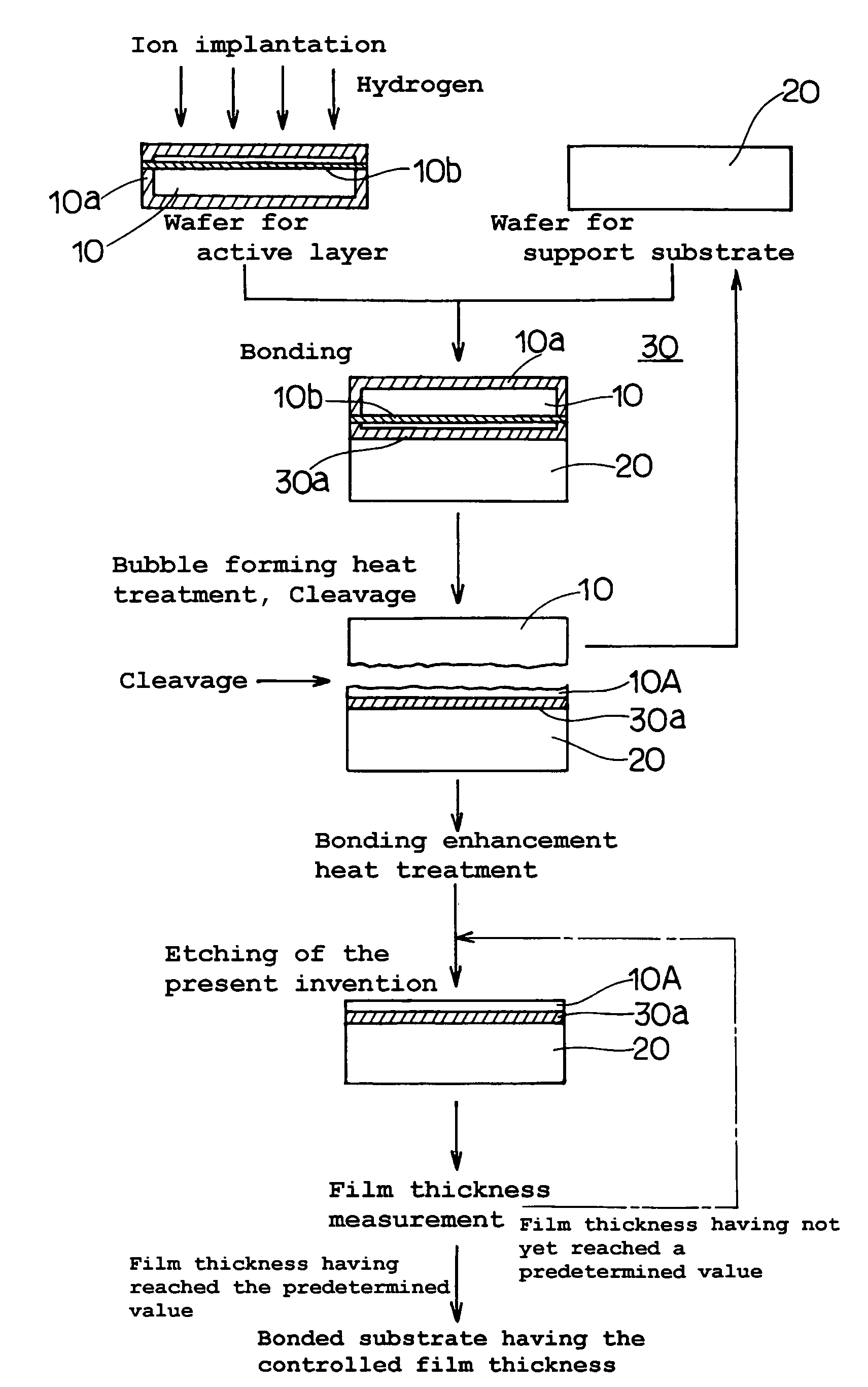
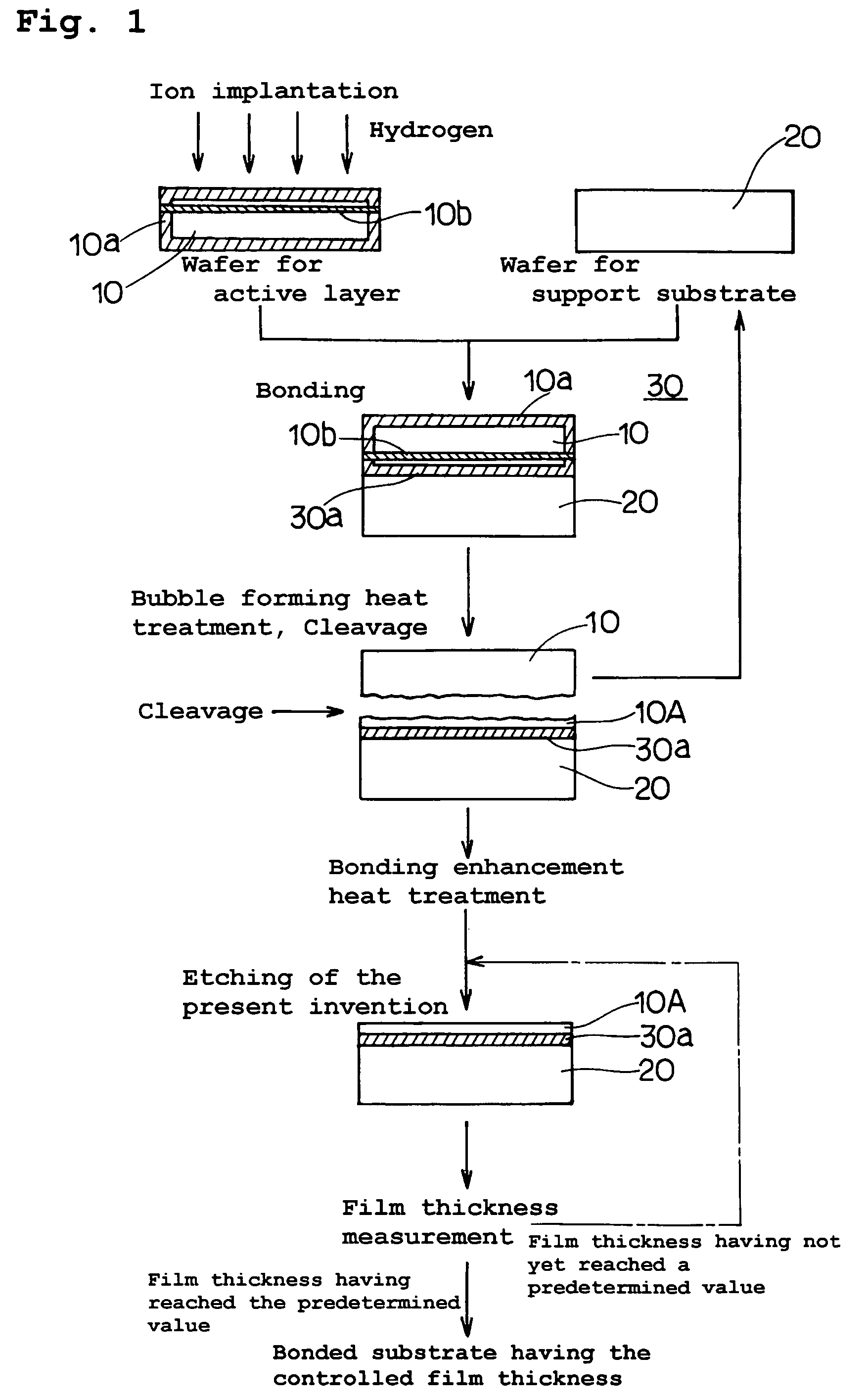
[0075]FIG. 1 is a flow chart showing a manufacturing method of a bonded substrate (SOI substrate) according to the present invention.

[0076]As shown in FIG. 1, firstly a wafer for active layer (silicon wafer) 10 is prepared by applying to a single-crystal silicon ingot that has been pulled up by the CZ method, each of the processes including slicing, beveling, lapping, etching and polishing so as to form it into a wafer having a thickness of 725 μm and a diameter of 200 mm (8 inches) with one-side or both-sides thereof mirror finished. On the other hand, a wafer for support substrate (silicon wafer) 20 is prepared by using the same manufacturing method as that used for the wafer for active layer 10 so as to be formed into a wafer having the same thickness and the same diameter as the wafer for active layer and a mirror finished surface. The active layer wafer 10 from those two is introduced into a thermal oxidation furnace, where it is treated with the thermal oxidation at 900° C. wh...

second embodiment

[0088]the present invention will now be described with reference to FIG. 2.

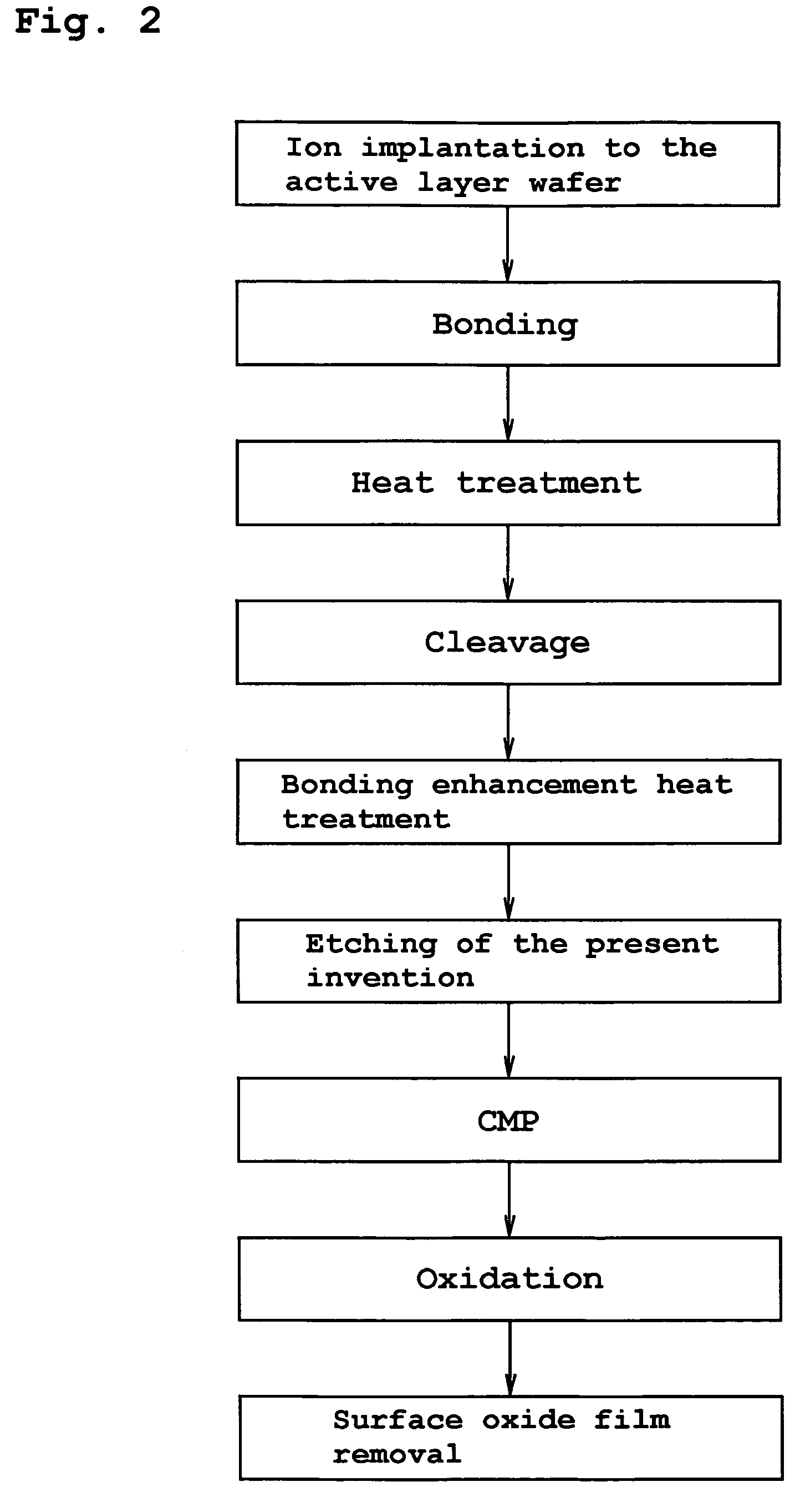
[0089]FIG. 2 is a flow chart showing a manufacturing method of a bonded substrate (SOI substrate) according to the second embodiment.

[0090]In the second embodiment, following to the same procedure as in the first embodiment, the process begins with the hydrogen ion implantation to the active layer wafer, then goes through the bonding of the active layer wafer with the support substrate wafer, the cleavage heat treatment for the bubble formation in the bonded wafer, the cleaving of the active layer wafer at its portion of the ion-implanted region, and the bonding heat treatment for enhancing the bonding strength of the bonded wafer, and finally provides the etching of the surface of the active layer by a predetermined amount by using the SC-1 cleaning fluid. This embodiment is specific in that subsequently the CMP process, the oxidation and the oxide film removal are sequentially applied to the surface of the ...

third embodiment

[0099]the present invention will now be described.

[0100]FIG. 3 is a flow chart showing a manufacturing method of a bonded substrate (SOI substrate) according to the third embodiment of the present invention.

[0101]In this embodiment, following to the same procedure as in the second embodiment, the process begins with the hydrogen ion implantation into the active layer wafer, then goes through the bonding of the active layer wafer with the support substrate wafer, the heat treatment for the bubble formation in the bonded wafer, the cleaving of the active layer wafer at its portion of the ion-implanted region, and the bonding heat treatment for enhancing the bonding strength of the bonded wafer, and finally provides the etching of the surface of the active layer by using the SC-1 cleaning fluid. This embodiment is specific in that subsequently the oxidation and the oxide film removal are sequentially applied to the surface of the active layer.

[0102]In this case, the surface roughness o...


PUM

PropertyMeasurementUnit
thicknessaaaaaaaaaa
pHaaaaaaaaaa
thicknessaaaaaaaaaa

Abstract

The present invention provides a bonded substrate fabricated to have its final active layer thickness of 200 nm or lower by performing the etching by only 1 nm to 1 μm with a solution having an etching effect on a surface of an active layer of a bonded substrate which has been prepared by bonding two substrates after one of them having been ion-implanted and then cleaving off a portion thereof by heat treatment. SC-1 solution is used for performing the etching. A polishing, a hydrogen annealing and a sacrificial oxidation may be respectively applied to the active layer before and / or after the etching. The film thickness of this active layer can be made uniform over the entire surface area and the surface roughness of the active layer can be reduced as well.

Description

[0001]This application is a 371 of international application PCT / JP2004 / 004886, which claims priority based on Japanese patent application No. 2003-099541 filed Apr. 2, 2003, which is incorporated herein by reference.FIELD OF THE INVENTION[0002]The present invention relates to a bonded semiconductor substrate and a manufacturing method thereof, and more particularly to such a bonded semiconductor substrate and a manufacturing method thereof that comprises an active layer formed by cleaving and separating a portion of an active layer substrate, specifically the semiconductor substrate having an uniform thickness of the active layer across an entire surface thereof without inducing any peel-off of the active layer, even if the active layer of thin film has the thickness as thin as 0.2 μm or lower.DESCRIPTION OF THE PRIOR ART[0003]The bonded semiconductor substrate has been broadly studied, especially in the field of semiconductors, from the viewpoint of its feature created by bonding ...

Claims


Application Information

Patent Timeline
Patent Type & Authority Patents(United States)
IPC IPC(8): B44C1/22H01L21/30H01L21/46C03C15/00C03C25/68H01L27/12H01L21/02H01L21/306H01L21/762
CPCH01L21/30608H01L21/76254H01L21/20H01L27/12
Inventor KAMIYAMA, EIJIKATOH, TAKEOPARK, JEA GUN
Owner SUMCO CORP
Learn More