Low power non-volatile memory and gate stack

a non-volatile memory, low-power technology, applied in the direction of semiconductor devices, electrical devices, nanotechnology, etc., can solve the problems of affecting the reliability of devices, affecting the characteristics of devices, and damage to device materials, etc., to achieve good charge retention, low voltage, and high charge blocking barriers

Active Publication Date: 2009-11-03
MICRON TECH INC
View PDF7 Cites 76 Cited by
  • Summary
  • Abstract
  • Description
  • Claims
  • Application Information

AI Technical Summary

Benefits of technology

[0011]Non-volatile memory devices and arrays, in accordance with embodiments of the present invention, utilize band-gap engineered gate stacks with asymmetric tunnel barriers in floating node memory cells that allow for low voltage direct tunneling programming and erase, while maintaining high charge blocking barriers and deep carrier trapping sites for good charge retention. This allows memory device embodiments of the present invention to operate with the characteristics of an ideal or universal memory device. The low voltage direct tunnel program and erase capability also reduces damage to the gate stack and the crystal lattice from high energy carriers, reducing write fatigue and leakage issues and enhancing device lifespan allowing effective infinite endurance (1012 to 1015 program / erase cycles). The low voltage program and erase of embodiments of the present invention also allow for low voltage memory array design and a smaller effective oxide thickness (EOT) of the memory cell gate-stacks, allowing low power, voltage scaling, and for an overall memory array die area reduction and enabling further scaling of device features as process technology improves. Reverse and normal mode memory cell embodiments of the present invention are detailed. Other memory cell embodiments of the present invention allow multiple levels of bit storage in a single memory cell. Embodiments of the present invention arranged in NOR or NAND memory architectures are also provided.

Problems solved by technology

Most RAM, such as dynamic RAM (DRAM), static RAM (SRAM) and synchronous DRAM (SDRAM), is volatile, which means that it requires a steady flow of electricity to maintain its contents.
As soon as the power is turned off, whatever data was in RAM is lost.
Both mechanisms require significant amounts of power and the generation of high positive and negative voltages in the memory device which can place high fields across the gate insulation layers with resulting adverse effects in device characteristics and reliability.
A problem with CHE, hot hole injection and Fowler-Nordheim tunneling is that the high energy required for their operation damages the device materials, reducing memory cell lifetimes and endurance.
They can also consume large amounts of power, which is a problem in portable devices.
In addition, the high voltages and fields limit the device feature scalability of the array and its support circuitry and significantly slow the write, read and erase speed of the resulting device.
Fowler-Nordheim tunneling and hot hole injection can generate fixed charge centers in the tunneling insulators and shallow traps and defects in the trapping layer, thus breaking stable bonds and eventually degrading the insulator / dielectric properties of the device (limiting device endurance to a typical lifetime of less than 106 program / erase cycles).
Such high power, high voltage, slow access speed, limited endurance and scaling difficulties are a typical characteristic of most commonly utilized non-volatile memory devices.

Method used


Image

  • Low power non-volatile memory and gate stack
  • Low power non-volatile memory and gate stack
  • Low power non-volatile memory and gate stack

Examples


Embodiment Construction

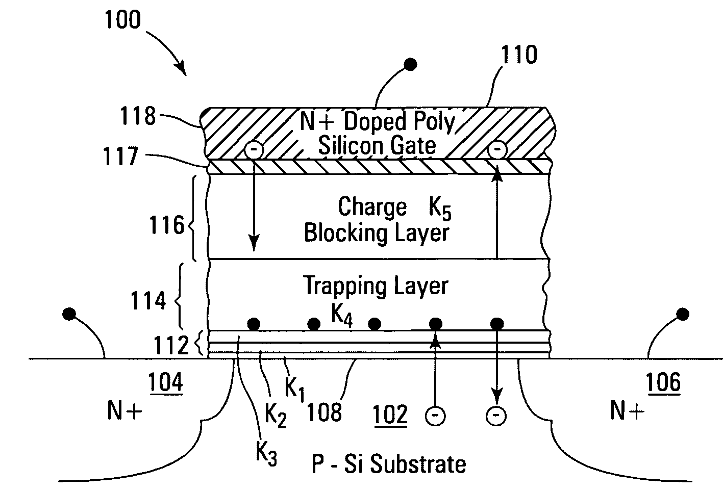
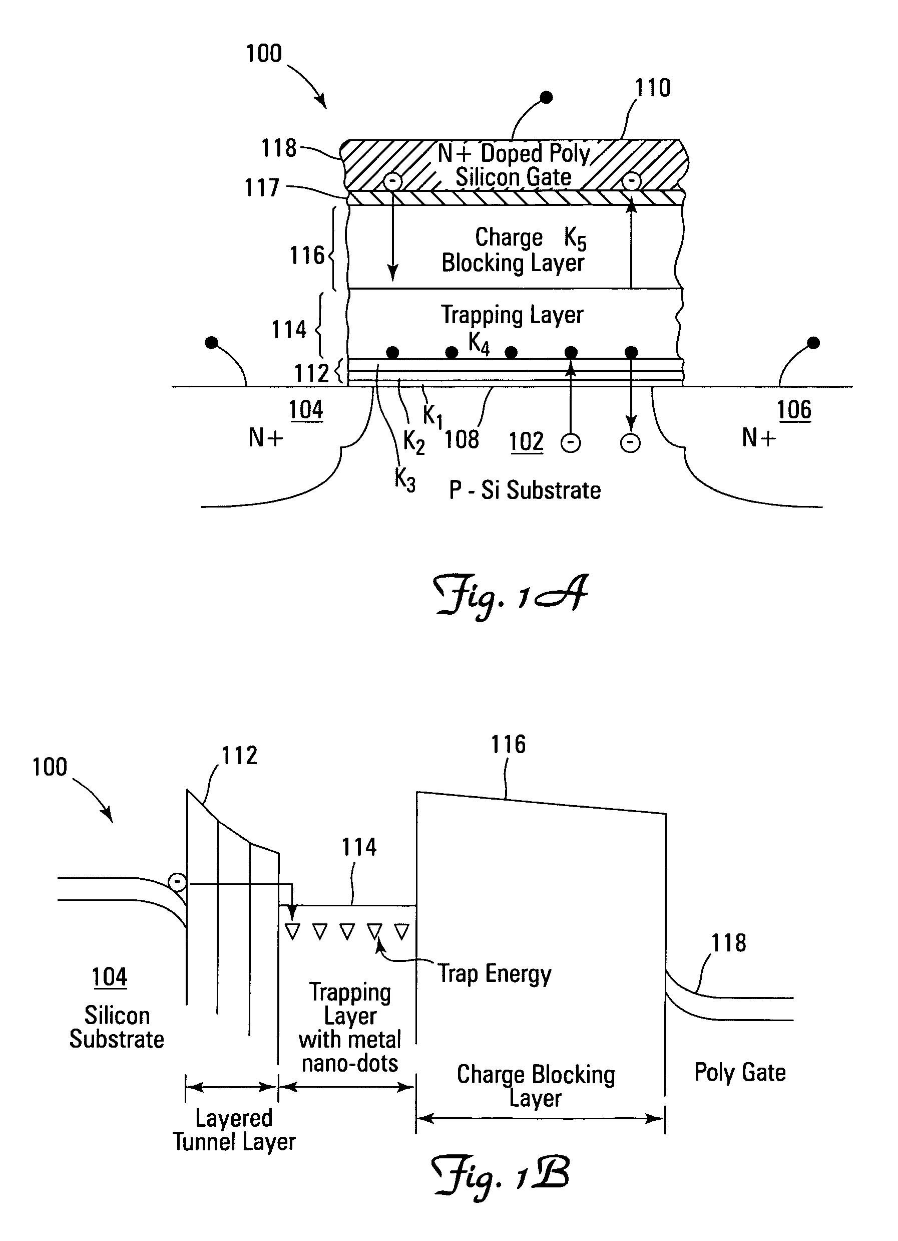
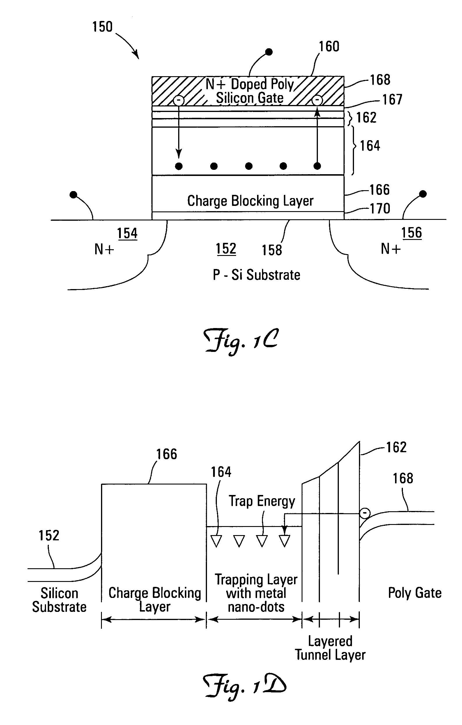
[0022]In the following detailed description of the preferred embodiments, reference is made to the accompanying drawings that form a part hereof, and in which is shown by way of illustration specific preferred embodiments in which the inventions may be practiced. These embodiments are described in sufficient detail to enable those skilled in the art to practice the invention, and it is to be understood that other embodiments may be utilized and that logical, mechanical and electrical changes may be made without departing from the spirit and scope of the present invention. The terms wafer and substrate used previously and in the following description include any base semiconductor structure. Both are to be understood as including silicon-on-sapphire (SOS) technology, silicon-on-insulator (SOI) technology, thin film transistor (TFT) technology, doped and undoped semiconductors, epitaxial layers of silicon supported by a base semiconductor, as well as other semiconductor structures wel...


PUM


Abstract

Non-volatile memory devices and arrays are described that facilitate the use of band-gap engineered gate stacks with asymmetric tunnel barriers in reverse and normal mode floating node memory cells in NOR or NAND memory architectures that allow for direct tunnel programming and erase, while maintaining high charge blocking barriers and deep carrier trapping sites for good charge retention. The low voltage direct tunneling program and erase capability reduces damage to the gate stack and the crystal lattice from high energy carriers, reducing write fatigue and enhancing device lifespan. The low voltage direct tunnel program and erase capability also enables size reduction through low voltage design and further device feature scaling. Memory cells of the present invention also allow multiple bit storage. These characteristics allow memory device embodiments of the present invention to operate within the definition of a universal memory, capable of replacing both DRAM and ROM in a system.

Description

TECHNICAL FIELD OF THE INVENTION [0001]The present invention relates generally to integrated circuits and in particular the present invention relates to non-volatile memory devices.BACKGROUND OF THE INVENTION [0002]Memory devices are typically provided as internal storage areas in the computer. The term memory identifies data storage that comes in the form of integrated circuit chips. There are several different types of memory used in modern electronics, one common type is RAM (random-access memory). RAM is characteristically found in use as main memory in a computer environment. RAM functions as a read and write memory; that is, you can both write data into RAM and read data from RAM. This is in contrast to read-only memory (ROM), which permits you only to read data. Most RAM, such as dynamic RAM (DRAM), static RAM (SRAM) and synchronous DRAM (SDRAM), is volatile, which means that it requires a steady flow of electricity to maintain its contents. As soon as the power is turned off...

Claims


Application Information

Patent Timeline
Patent Type & Authority Patents(United States)
IPC IPC(8): H01L29/788
CPCB82Y10/00H01L29/42332H01L29/7881H01L29/792H01L29/513Y10S438/954H10B99/00
Inventor BHATTACHARYYA, ARUP
Owner MICRON TECH INC
Why Eureka
Try Eureka