Front-side illuminated, back-side contact double-sided PN-junction photodiode arrays

a photodiode array and back-side contact technology, applied in the field of thin wafer photodiodes, can solve the problems of negating the benefits of the smaller device size, difficult to provide efficient interconnection between devices, and unmatched user-friendliness, and achieve the effect of maintaining the overall performance characteristics of the photodiode array and individual diode units

Active Publication Date: 2010-02-02
UDT SENSORS +1
View PDF80 Cites 24 Cited by
  • Summary
  • Abstract
  • Description
  • Claims
  • Application Information

AI Technical Summary

Benefits of technology

[0018]The present invention describes several embodiments of a novel photodiode array and methods making the novel photodiode arrays that can be feasibly fabricated using thin wafers while still maintaining the overall performance characteristics of the photodiode array and individual diode units. More specifically, the photodiode arrays of the present invention have PN-junctions that are electrically connected from the front to back surfaces, and thus, can be operated in a fully depleted mode at low reverse bias.

Problems solved by technology

Silicon photodiodes, essentially active solid-state semiconductor devices, are among the most popular photodetectors coalescing high performance over a wide wavelength range with unmatched user-friendliness.
As the devices become smaller, however, it becomes more difficult to provide efficient interconnections between devices, thus negating the benefits of the smaller device size.
In addition to the high cost of manufacturing and low throughput, another typical problem with high-density integration of conventional photodiode arrays is the amount and extent of crosstalk that occurs between adjacent detector structures, primarily as a result of minority carrier current between diodes.
However, at conventional doping levels utilized for diode arrays of this type, the diffusion length of minority carriers generated by photon interaction in the semiconductor is in the range of at least many tens of microns, and such minority carriers have the potential to affect signals at diodes away from the region at which the minority carriers were generated.
Therefore, the spatial resolution obtainable may be limited by diffusion of the carriers within the semiconductor itself, even if other components of the optical system are optimized and scattered light is reduced.
It is difficult, however, to generate thin wafer photodiodes in which leakage current and noise is controlled and the wafer is sufficiently sturdy to handle processing and use is difficult.
The production of such arrays is often plagued by excessive loss due to breakage of the delicate thin wafers.
In addition, as photodiode detector devices become smaller, it becomes more difficult to provide efficient interconnections between devices, thus putting an additional demand on device electrical requirements.
Multiple level metallization creates planarity problems in the metallization layers, however, thereby limiting interconnection density.
The prior art, however, fails to provide a thin wafer photodiode structure and method of manufacturing that produces sufficiently sturdy wafers while still maintaining the overall performance characteristics of photodiode arrays and their individual diode units, within detection systems.
Using conventional technology, a photodiode array fabricated on bulk silicon material cannot be fully depleted at 5 volts.
While it is easy to fully deplete a device at high bias, it is almost impossible to fully deplete a bulk silicon device at very low bias.

Method used


Image

  • Front-side illuminated, back-side contact double-sided PN-junction photodiode arrays
  • Front-side illuminated, back-side contact double-sided PN-junction photodiode arrays
  • Front-side illuminated, back-side contact double-sided PN-junction photodiode arrays

Examples


first embodiment

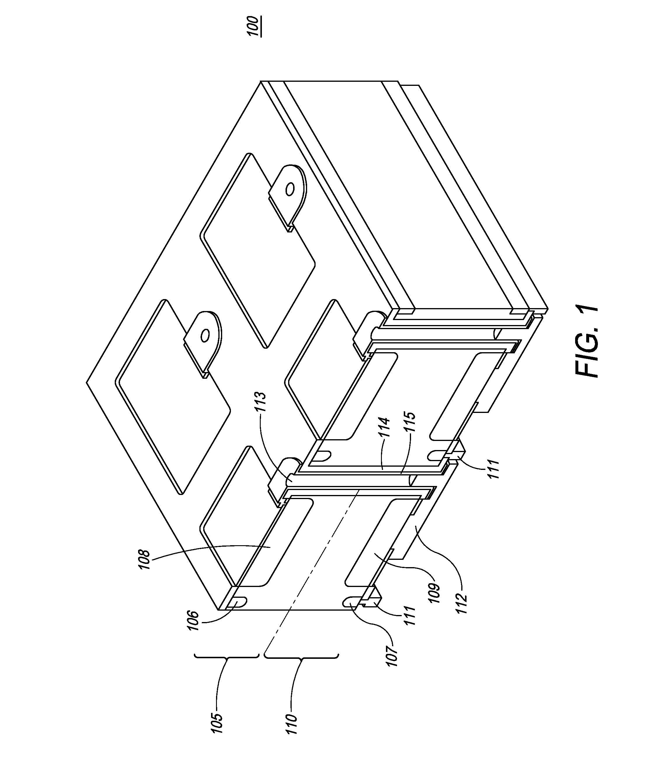
[0038]FIG. 1 is a cross-sectional view of a front-side illuminated, back-side contact (FSL-BSC) double-sided PN-junction photodiode array formed in accordance with the present invention. In one embodiment, photodiode array 100 is preferably formed from a device wafer of suitable semiconductor material. For example, but, not limited to such example, a silicon wafer is used as the starting material for the photodiode array of the present invention. In one embodiment, the starting material is a silicon wafer having the following specifications: a 6-inch diameter; a thickness ranging from 0.210-0.260 mm; n-type conductivity; and a resistivity on the order of 8000 Ωcm. In another embodiment, the starting material is a silicon wafer having the following specifications: a 5-inch diameter; a thickness ranging from 0.210-0.260 mm; n-type conductivity; and a resistivity on the order of 8000 Ωcm. The above specifications are merely for the purposes of illustration, and are not limiting. Conseq...

second embodiment

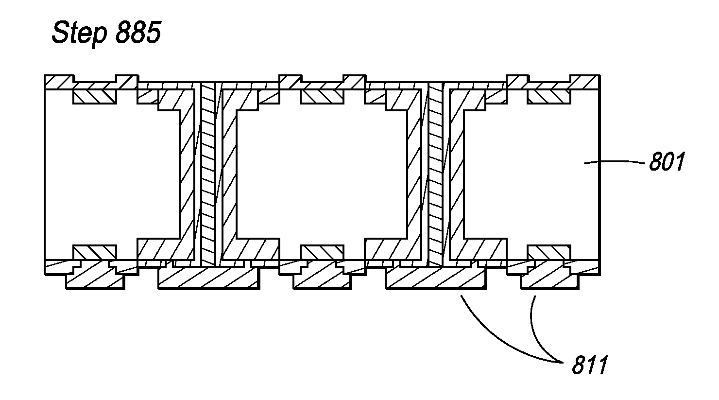
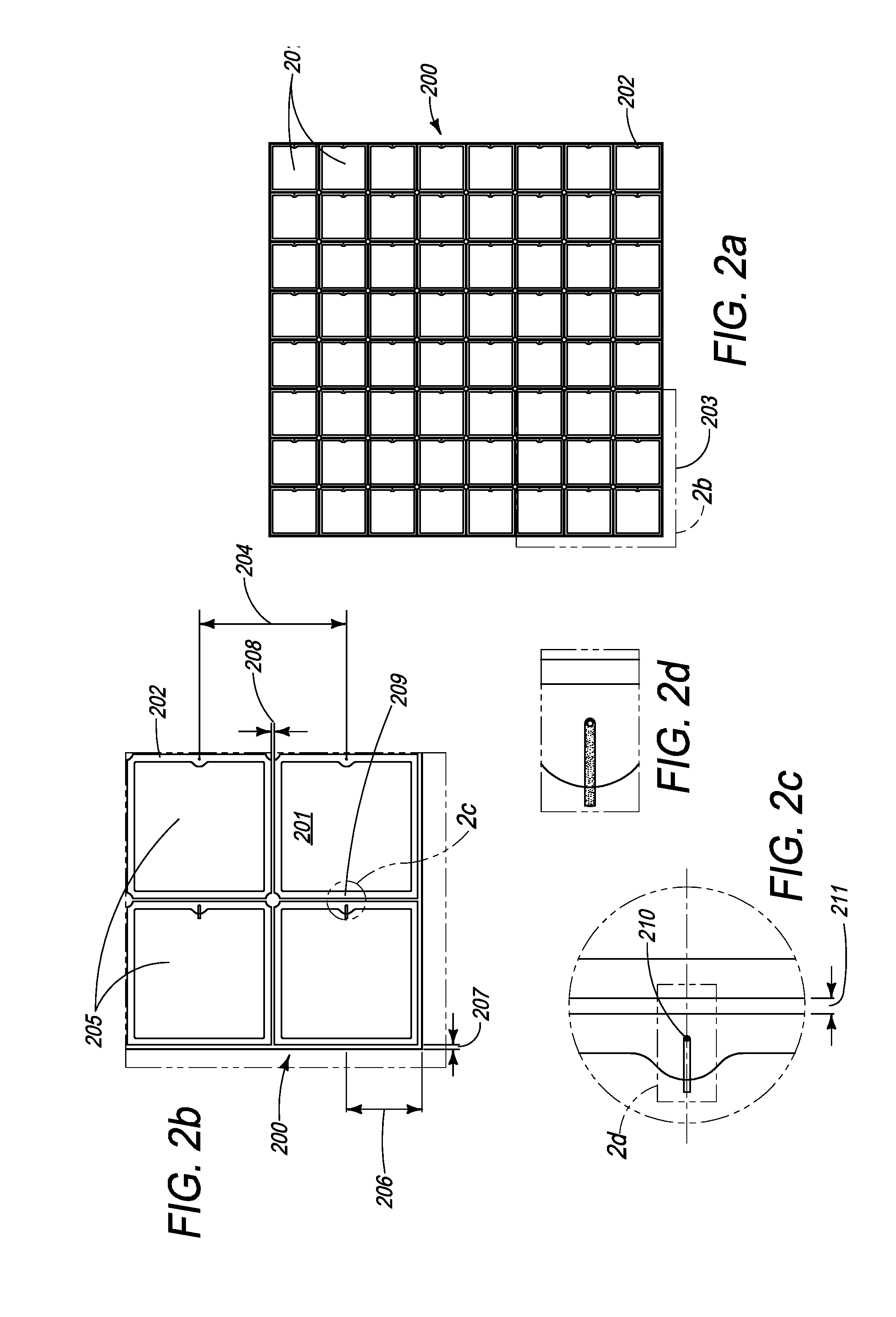
[0080]For example, but not limited to such example, if regions 506, 507, 508, and 509 are doped with a suitable impurity of a first conductivity type wherein the first conductivity type is n-type, then regions 511a, 511b, 511c, 511d, 511e, and 511f are doped with a suitable impurity of a second conductivity type, wherein the second conductivity type is p-type. The second embodiment will be described with respect to this scenario, but it should be noted herein that the photodiode array of the present invention and method of manufacturing the same is not limited to the embodiment described herein.

[0081]In one embodiment, the present invention comprises PN-junctions on both front and back sides of the wafer. While boron (B) and phosphorus (P) are the preferred p-type and n-type dopants employed to create the p+ and n+ regions, it should be understood to those of ordinary skill in the art that any suitable doping material may be used. Preferably, doped diffusion regions 511a, 511b, 511e...


PUM


Abstract

The present invention is a photodiode detector array for use in computerized tomography (CT) and non-CT applications. Specifically, the present invention is a high-density photodiode arrays, with low dark current, low capacitance, high signal to noise ratio, high speed, and low crosstalk that can be fabricated on relatively large substrate wafers. More specifically the photodiode array of the present invention is fabricated such that the PN-junctions are located on both the front side and back side surfaces of the array, and wherein the front side PN-junction is in electrical communication with the back side PN-junction. Still more specifically, the present invention is a photodiode array having PN-junctions that are electrically connected from the front to back surfaces and which can be operated in a fully depleted mode at low reverse bias.

Description

FIELD OF THE INVENTION[0001]The present invention is directed towards thin wafer photodiodes having improved strength and handling characteristics. Specifically, the present invention is directed towards novel photodiodes and methods of making novel photodiodes that can be feasibly fabricated using thin wafers while still maintaining the overall performance characteristics of the photodiode array and individual diode units. Still more specifically, the photodiode arrays of the present invention have PN-junctions that are electrically connected from the front to back surfaces, and thus, can be operated in a fully depleted mode at low reverse bias.BACKGROUND OF THE INVENTION[0002]Photodiodes are typified by the quantification of certain characteristics, such as electrical, optical, current (I), voltage (V), and noise. Electrical characteristics predominantly include shunt resistance, series resistance, junction capacitance, rise or fall time and frequency response whereas optical char...

Claims


Application Information

Patent Timeline
Patent Type & Authority Patents(United States)
IPC IPC(8): H01L31/06
CPCH01L27/1443H01L27/1446H01L27/1463H01L27/14645H01L31/0352H01L31/103H01L31/115Y02E10/547
Inventor BUI, PETER STEVENTANEJA, NARAYAN DASS
Owner UDT SENSORS
Why Eureka
Try Eureka