Optical component assembly

a technology of optical components and components, applied in the direction of instruments, semiconductor laser structural details, lasers, etc., can solve the problem that the wire bond can act as an unwanted aerial, and achieve the effect of improving flexibility in electrical connection, and reducing the risk of interferen

Inactive Publication Date: 2010-02-16
OPTITUNE
View PDF18 Cites 8 Cited by
  • Summary
  • Abstract
  • Description
  • Claims
  • Application Information

AI Technical Summary

Benefits of technology

[0036]The combination of a laser diode and a planar waveguide as the first and second components is likely to be a particularly useful one since the waveguide can be used to direct the output of the laser to another component or components, such as an optical fibre or a modulator. Further, the waveguide can act as an external cavity for the laser diode, thus for example narrowing its linewidth.
[0037]Packaging, assembly and alignment of optical components and systems can potentially become easier, cheaper and / or more reliable by using an embodiment of the present invention. Embodiments of the present invention are particularly suitable for packaging and integration of optoelectronic components at wafer-level.
[0038]An advantage of embodiments of the present invention is an increased flexibility in making electrical connection to optoelectronic components. Not only can wire bonds be used, for instance from a device to contact pads on a substrate, but connection can also or alternatively be made through the mounting by using a conductive material at the mounting interface to the shared substrate, together with contact pads or areas on the shared substrate.

Problems solved by technology

For example, for high speed devices it has been found that wire bonds can act as an unwanted aerial.

Method used


Image

  • Optical component assembly
  • Optical component assembly
  • Optical component assembly

Examples


worked example

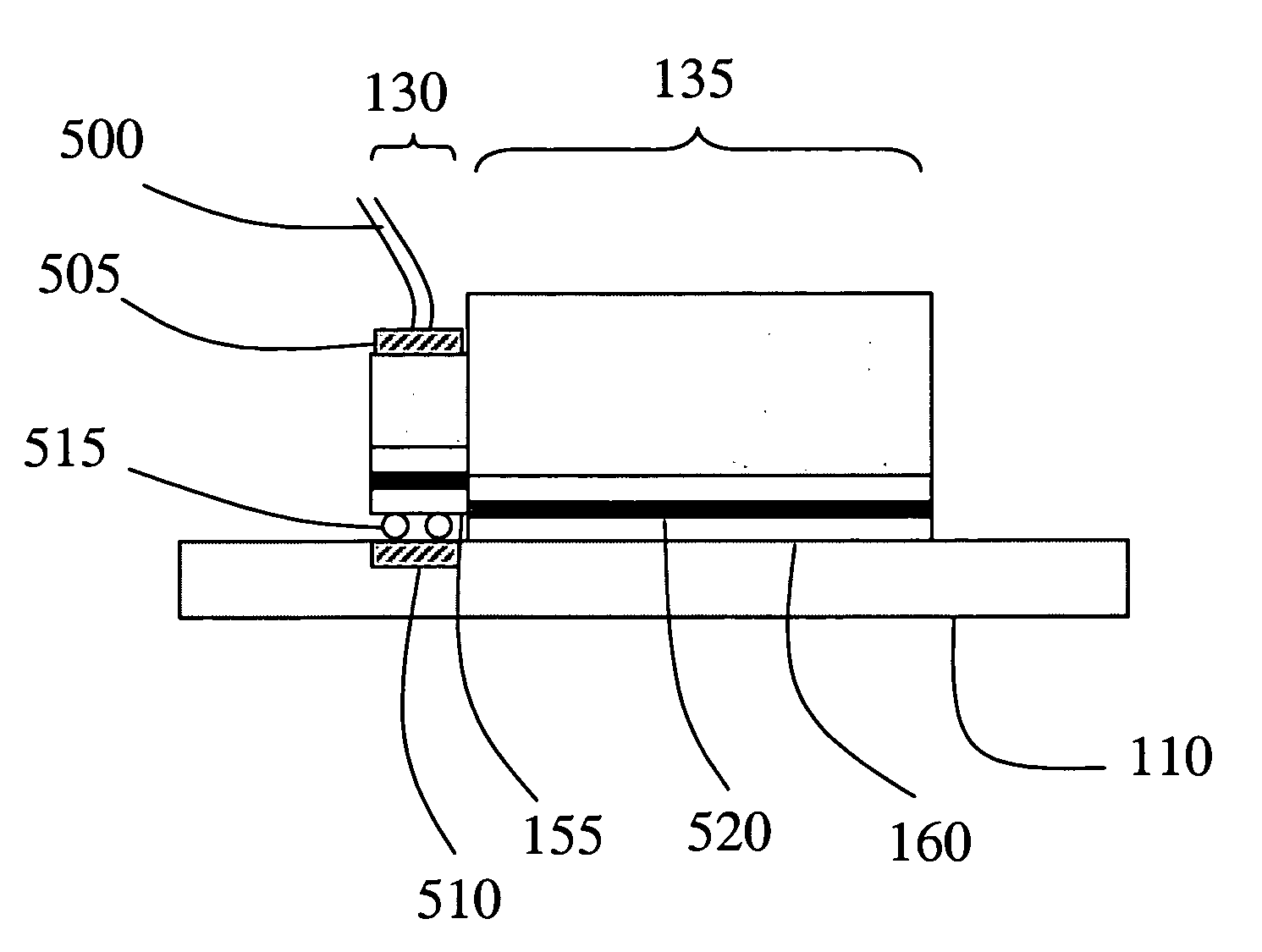
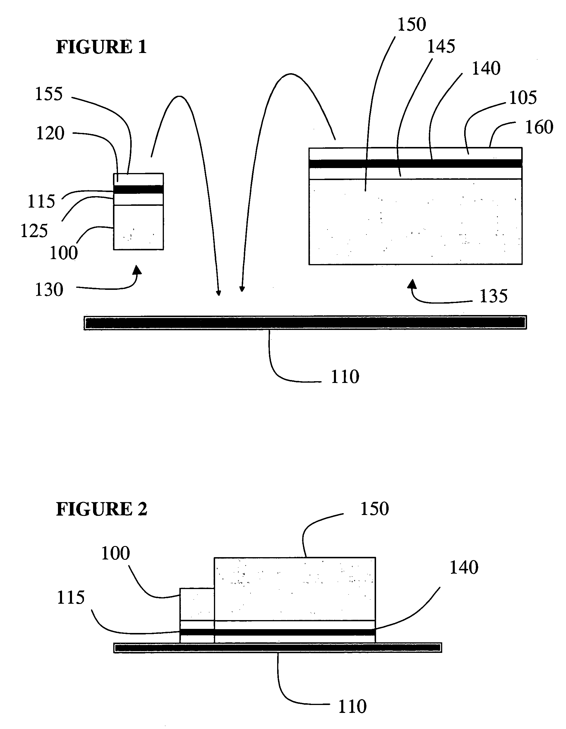
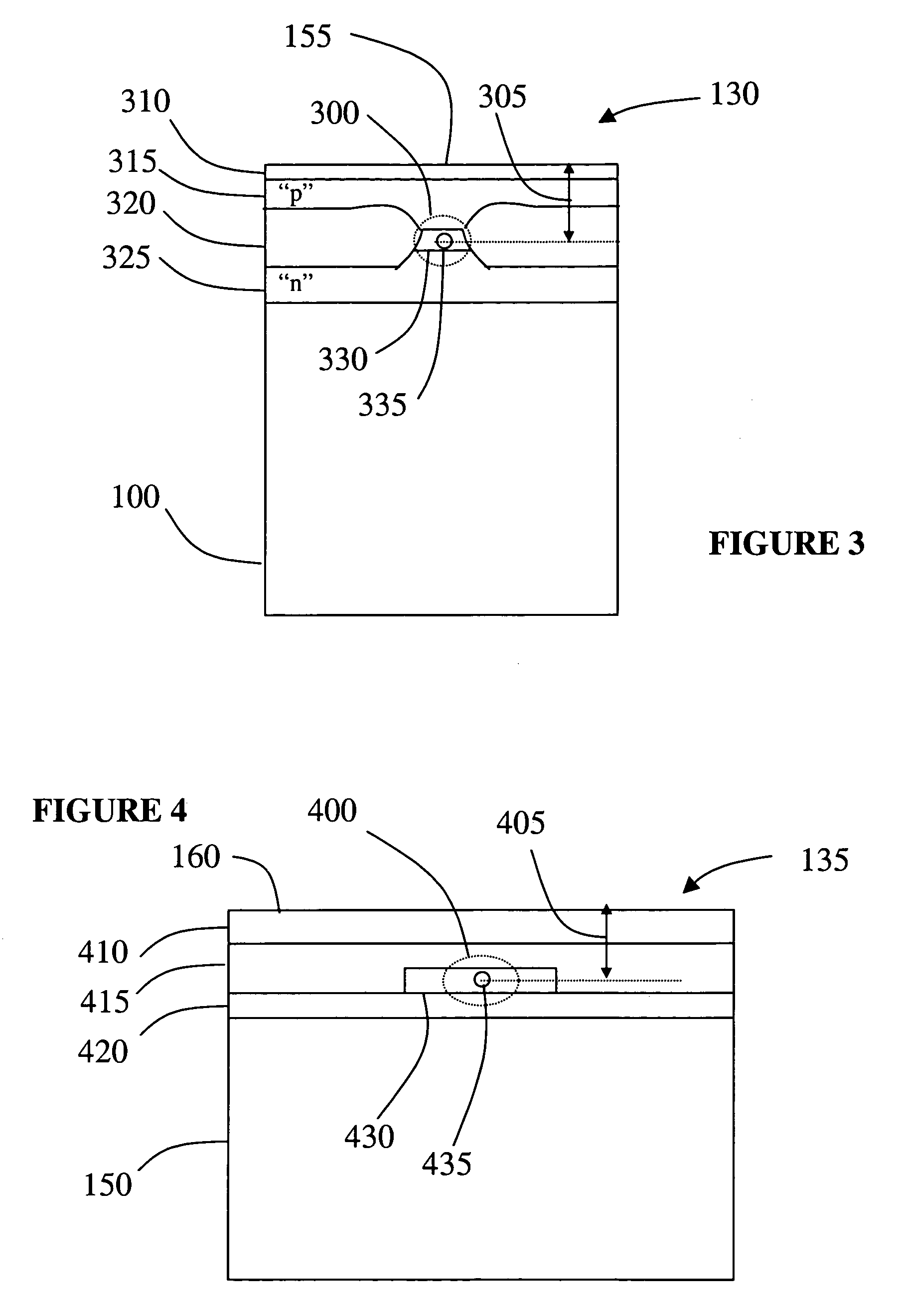
[0116]The following describes materials and planar fabrication techniques for fabricating a waveguide device 135 of the type shown in FIGS. 1 and 2 and flip chip mounting it on a substrate 110 in optical alignment with a laser diode 130.

[0117]The cladding layers 145, 105 are a composition of 0.1 mol of vinyltrichlorosilane and 0.1 mol of phenyltrichlorosilane. This composition gives a refractive index after final film annealing at 230 deg C. of 1.5060 at 1552 nm wavelength. The synthesis of the cladding layers 145, 105 is based on hydrolysis and polycondensation reactions. The viscous raw material is diluted into a methylisobutylketone (MIBK) solvent so that the viscosity of the material is 150 mPas. A thermal initiator is added to enhance thermal crosslinking of the vinyl groups. The core layer 140 has the same composition as the cladding layers 145, 105 but is doped with 2% germanium chloride so that its refractive index is 1.5100 at 1552 nm wavelength after final annealing at 235...


PUM


Abstract

Optical components are flip chip mounted onto a substrate for improved alignment. Each device is fabricated using “build-up” layers above a substrate. Each has an optical confinement region in which optical radiation travels in use, and a bonding surface. The overall depth of the layers above the optical confinement region is closely controlled during fabrication, for instance by the use a “spacer” layer, so that when the devices are subsequently flip chip mounted adjacent one another on a shared substrate by means of their bonding surfaces, they can be passively positioned so that their optical confinement regions abut and optical radiation can be coupled from one to the next in use.

Description

CROSS REFERENCE TO RELATED APPLICATION[0001]This application claims priority from GB application No. 225,522.2 filed Nov. 1, 2002.BACKGROUND[0002]1. Technical Field of Exemplary Embodiments of the Present Invention[0003]The present invention relates to mounted optical components and finds particular application where two or more optical components are mounted for optical alignment.[0004]2. Description of Related Art[0005]Flip chip mounting is known for use in mounting semiconductor devices. It is also known for use in mounting optical devices. Reference can be made for example to U.S. Pat. Nos. 5,478,778 and 6,316,281 and to European patent application number 0642045. The technique comprises fabricating a planar device and then inverting it onto a bonding area on a substrate. Bonding material applied to the bonding area can also be used to make an electrical connection to the device and this has advantages in some circumstances over the older technique of wire bonding. For example, ...

Claims


Application Information

Patent Timeline
Patent Type & Authority Patents(United States)
IPC IPC(8): H01L23/495G02B6/42H01S5/02H01S5/022
CPCG02B6/423G02B6/4232H01S5/0224H01S5/02252H01S5/02272H01L2924/0002H01S5/02284H01L2924/00H01S5/02326H01S5/0237H01S5/0234H01S5/02251
Inventor KARKKAINEN, ARI
Owner OPTITUNE
Why Eureka
Try Eureka