Superlattice photodiodes with polyimide surface passivation

a surface passivation and photodiode technology, applied in the field of infrared focal plane arrays, can solve the problems of poor uniformity, high cost and complex process of molecular beam epitaxy, and increase the surface resistivity of polyimide passivated photodiodes

Active Publication Date: 2010-03-23
NORTHWESTERN UNIV
View PDF1 Cites 11 Cited by
  • Summary
  • Abstract
  • Description
  • Claims
  • Application Information

AI Technical Summary

Benefits of technology

[0016]The subject invention comprises a superlattice photodiode with polyimide surface passivation. Nearly bulk-limited electrical performance in type-II InAs / GaSb superlattice photodiodes can be achieved with proper surface preparation followed by polyimide encapsulation, while also providing physical protection of the underlying semiconductor. The surface resistivity of polyimide passivated photodiodes can be increased at least one order of magnitude compared to as-processed devices. This process has been demonstrated to be compatible with mesa dimensions and pitches found in typical FPA fabrication processes. The polyimide passivation can be shown to be stable upon exposure to various ambient conditions, as well as over time. This passivation technique has promising implications for the practical realization of infrared imaging sensors based on type-II InAs / GaSb superlattices.

Problems solved by technology

While each of the above processes are viable, certain disadvantages exist; for example, LPE experiences growth problems with InAsSbP alloys and potential nonuniform growth as well as melt-back effect.
Molecular-beam epitaxy is a very expensive and complex process, and difficulties have been reported with p-type doping and with the growth of phosphorus-bearing alloys.
Vapor-phase epitaxy disadvantages include potential for hillock and haze formation and interfacial decomposition during the preheat stage.
However, the properties of SiO2 film often leads to poor uniformity and film adhesion problems during processing.
The disadvantages are the much higher capitol equipment cost and, to a lesser extent, the question of damage in the semiconductor surface.
The fabrication of index guided InAsSbP / InAsSb / InAs lasers is usually complicated and requires several stages.
However, its performances are limited between 8 and 12 μm by its RoA and the absence of a passivation technique with the ability to efficiently protect the sample from degrading due to the aggressive steps in the Focal Plane Array (FPA) fabrication.
Several passivation techniques have been proposed, but all of them present significant disadvantages.
Sulfide based passivation layers are too thin and volatile to mechanically protect the diodes.
Epitaxial overgrowth of wide band gap AlxGa1-xAsySb1-y is complex and expensive.
In the proximity of the mesa sidewalls, this bending can provoke an accumulation of charges, eventually leading to a local inversion of the majority carriers in the superlattice.
This may result in the creation of a strong current along the sidewalls, shorting the p-n junctions.
The surface passivation of type-II InAs / GaSb superlattice photodiodes has been a limiting factor to the incorporation of this technology in infrared imaging systems and has been a known process technology challenge for a number of years.
The narrow band gap of long-wavelength infrared (LWIR) photodiodes and a highly reactive surface lead to Fermi level pinning at the surface of type-II sperlattice mesa diodes, resulting in deleterious surface-related tunneling currents and reduces, zero-biad detector impedance.
The chalcogen-based passivation, though initially effective, does not address the practical issue of physical protection and encapsulation of the device, and there have been reports of the temporal instability of such a passivation layer.
Dielectric passivation or type-II superlattice photodiodes presents the challenge of developing high-quality, low-fixed, and interfacial charge density dielectrics at process temperatures substantially below the material growth temperature, such that superlattice period intermixing does not occur.
This technique, however, requires very careful surface cleaning and preparation prior to the regrowth step and its feasibility in very high fill-factor focal plane arrays (FPAs) has not been demonstrated.

Method used


Image

  • Superlattice photodiodes with polyimide surface passivation
  • Superlattice photodiodes with polyimide surface passivation
  • Superlattice photodiodes with polyimide surface passivation

Examples


example

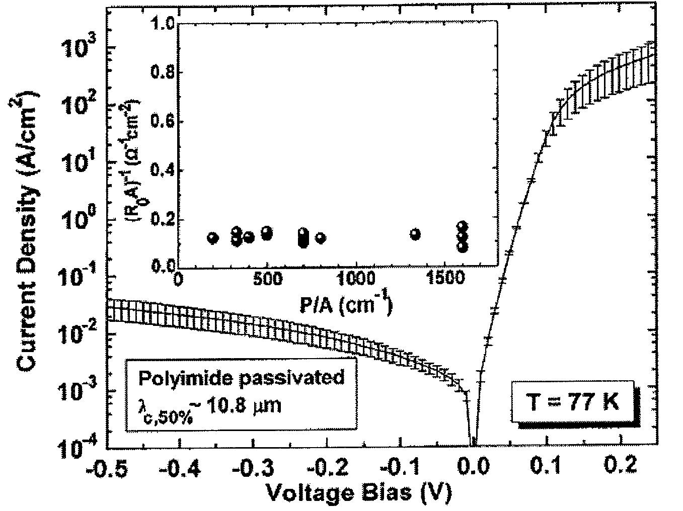
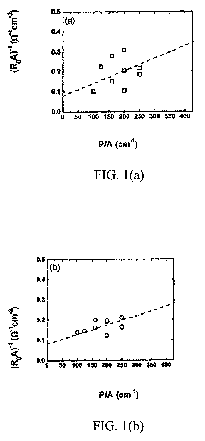
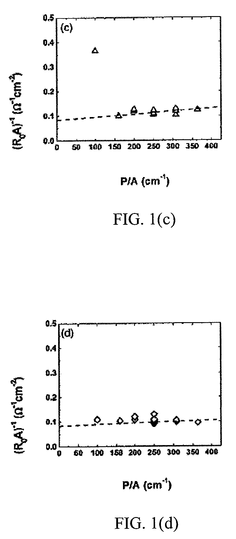
[0025]FIG. 1(a) shows a plot of the inverse of the zero-bias resistance area product versus the perimeter to area ratio for unpassivated diodes (sample A), measured immediately after the last cleaning step of the fabrication process. A considerable degree of nonuniformity in the RoA value at 77 K was observed. A linear least squares fitting (LLSF) was conducted while fixing the bulk RoA value (P / A=0) to 12.4 Ω·cm2, as extracted from a LLSF of a more uniform distribution of experimental values [FIG. 1(c)]. The surface resistivity was extracted to be 1.6×10³ Ωcm.

[0026]The same sample was then warmed to room temperature and allowed to remain under a vacuum of approximately 10−3 Torr, for 12 hours, after which time it was cooled to 77 K and measured again (sample B). FIG. 1(b) shows the resulting (RoA)−1 values. The fitting of these data resulted in a slightly higher surface resistivity of 2.1×10³ Ωcm than the as-processed sample, and the standard deviation of the RoA values decreased...


PUM


Abstract

The subject invention comprises the realization of a superlattice photodiode with polyimide surface passivation. Effective surface passivation of type-II InAs / GaSb superlattice photodiodes with cutoff wavelengths in the long-wavelength infrared is presented. A stable passivation layer, the electrical properties of which do not change as a function of the ambient environment, nor time, can be realized by a solvent-based surface preparation, vacuum desorption, and the application of an insulating polyimide layer.

Description

[0001]This invention was made with Government support under Contract Nos. HQ0006-06-C-7325, HQ0006-06-C-7517 and HQ0006-07-C-7656 awarded by the Missile Defense Agency. The Government has certain rights in the invention.BACKGROUND OF THE INVENTION[0002]This application relates to Infrared Focal Plane Arrays, and more particularly, to a method for surface passivation that is resistant to aggressive processes. Focal plane array fabrication requires a well passivated material that is resistant to aggressive processes. Type-II InAs / GaSb superlattice heterodiodes have the ability to be more resilient than homo-junction diodes in improving sidewall resistivity through the use of various passivation techniques.[0003]The growth of semiconductor III-V compounds by chemical vapor deposition (CVD) using organometallics and hydrides as elemental sources has recently developed into a viable process with many potential commercial applications. The metallo-organic chemical vapor deposition (MOCVD)...

Claims


Application Information

Patent Timeline
Patent Type & Authority Patents(United States)
IPC IPC(8): H01L21/00H01L29/00
CPCH01L27/14649H01L31/1868Y02E10/50
Inventor RAZEGHI, MANIJEH
Owner NORTHWESTERN UNIV
Why Eureka
Try Eureka