Backside illuminated imaging device, semiconductor substrate, imaging apparatus and method for manufacturing backside illuminated imaging device

a technology of illumination imaging and semiconductor substrates, which is applied in the direction of material analysis, radio frequency controlled devices, instruments, etc., can solve the problems of insufficient size of each constituent element, interference of the wiring portion of the wiring layer, and difficulty in keeping a saturation signal amount, so as to prevent an increase in dark current, stabilize the gettering capability, and high-quality image pickup

Inactive Publication Date: 2010-08-24
FUJIFILM CORP
View PDF24 Cites 18 Cited by
  • Summary
  • Abstract
  • Description
  • Claims
  • Application Information

AI Technical Summary

Benefits of technology

[0026]A first object of an illustrative, non-limiting embodiment of the invention is to provide a backside illuminated imaging device having an overflow drain structure advantageous to miniaturization that can prevent the degradation of blue sensitivity.
[0027]A second object of an illustrative, non-limiting embodiment of the invention is to provide a backside illuminated imaging device having an overflow drain structure advantageous to miniaturization that can prevent the degradation of blue sensitivity and can completely discharge unnecessary charges or realize an electronic shutter function having reduced fixed pattern noise.
[0028]A third object of an illustrative, non-limiting embodiment of the invention is to provide a backside illuminated imaging device capable of surely realizing a signal charge separation between different photoelectric conversion regions even when a depletion layer of the photoelectric conversion region is thick.

Problems solved by technology

A wiring portion of the wiring layer interferes with transmission of light incident into each photoelectric conversion portion.
When signal charges accumulated in this depth are read out from a CCD or CMOS formed in the semiconductor substrate surface, there is a difficulty since a problem of a residual image or the like occurs.
Since a drain region is arranged adjacent and parallel to each photoelectric conversion element in the horizontal type overflow drain structure, a size of each constituent element may not sufficiently increase when miniaturization is carried out in this structure, such that it is difficult to keep a saturation signal amount (or to improve the sensitivity).
As a result, the imaging device has a remarkable low blue sensitivity.
However, since a drain region is not provided above a position separated from a maximum potential point of a photodiode, excessive charges may not be sufficiently discharged.
Specifically, when an electronic shutter function is realized by discharging all electric charges accumulated in the photodiode, fixed pattern noise or the like is caused by electric charges residual in the photodiode when the electronic shutter is turned on.
Incidentally, a defect of a semiconductor device occurs due to contamination by heavy metal during a fabrication process, such that a device property may be deteriorated or reliability may be degraded.
Since an image sensor is very sensitive to noise occurring due to a dark current, sufficient light shielding is required, but the dark current is apt to increase also in contamination by heavy metal.
Accordingly, when the frontside illuminated type imaging device is manufactured, “backside gettering” to be conventionally performed may not be applied, such that there is a high possibility that the required sufficient gettering property is not obtained.
Accordingly, there is a high possibility that the gettering side becomes a dark current source, that is, a noise source.

Method used


Image

  • Backside illuminated imaging device, semiconductor substrate, imaging apparatus and method for manufacturing backside illuminated imaging device
  • Backside illuminated imaging device, semiconductor substrate, imaging apparatus and method for manufacturing backside illuminated imaging device
  • Backside illuminated imaging device, semiconductor substrate, imaging apparatus and method for manufacturing backside illuminated imaging device

Examples


specific example 1

[0426]Temperature: 300 ti 500° C.

[0427]Pressure: 100 to 200 Pa

[0428]Used Gases: Ar / O2 / H2 (of a mixture ratio of 100 / 1 / 1)

[0429]In the above conditions, oxygen gas is plasmanized with microwaves. Accordingly, the oxygen gas becomes highly active oxygen radical and sacrificial oxidation can be performed in the vicinity of the surface on which the SOI substrate is exposed. Actually, a high-quality oxide film having a film thickness of 10 nm is generated by radiating the microwaves for 150 seconds. However, the gases other than oxygen of the available gases are not essential. Argon (Ar) is an inactive carrier gas and hydrogen is used for the purpose of promoting oxidation.

[0430]Since oxidation is performed in only a reaction rate control region also for the highly active oxygen radical, a range up to a film thickness of 10 nm is a practical region in the low-temperature oxidation treatment. When an oxide film of more than the film thickness of 10 nm is formed, productivity is lowered sin...

specific example 2

[0431]Temperature: 400° C.

[0432]Pressure: 100 to 200 Pa

[0433]Used Gas: High-concentration ozone

[0434]In the above conditions, the low-temperature oxidation treatment is performed. Also in this case, a practical thickness range of a film to be formed is about 10 nm.

[0435]In the next step S16 as shown in FIG. 30, the low-temperature oxide film 75 of the surface (see FIG. 34(b)) formed in step S15 is removed (Fifth Step). For example, the low-temperature oxide film can be removed by performing a fluorine-nitric acid treatment or the like. That is, since the low-temperature oxide film 75 contains the gettering layer contaminated by heavy metal, the contaminated layer can be completely removed by exfoliating a total of the low-temperature oxide film 75. The resulting state is shown in FIG. 35(a).

[0436]In the next step S17 as shown in FIG. 30, another low-temperature oxidation treatment is performed in the vicinity of the surface on which the SOI substrate is exposed. An uncontaminated cl...


PUM


Abstract

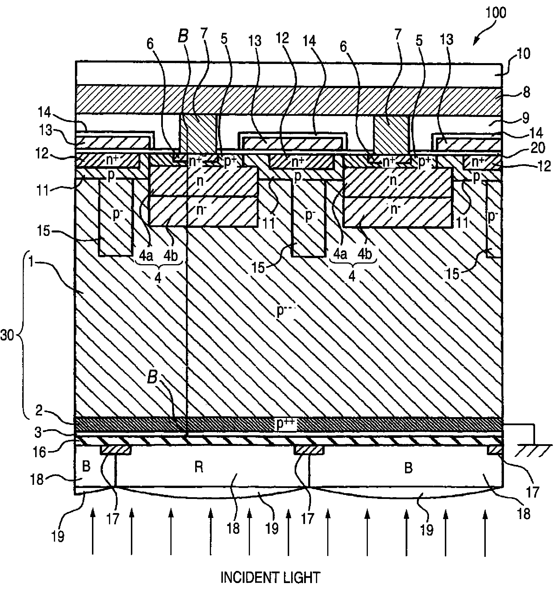
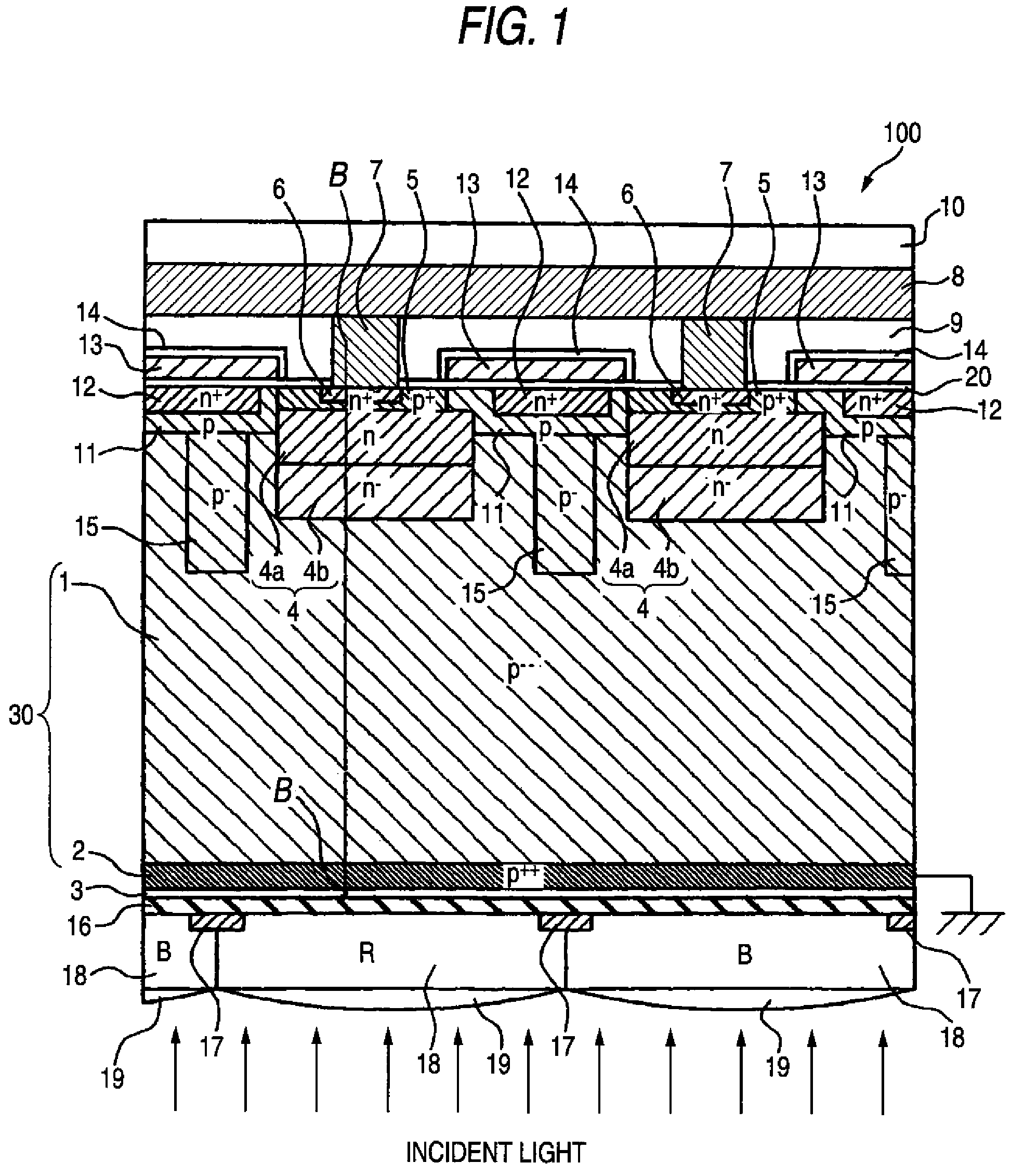
A backside illuminated imaging device performs imaging by illuminating light from a back side of a p substrate to generate electric charges in the substrate based on the light and reading out the electric charges from a front side of the substrate. The device includes n layers located in the substrate and on an identical plane near a front side surface of the substrate and accumulating the electric charges; n+ layers between the respective n layers and the front side of the substrate, the n+ layers having an exposed surface exposed on the front side surface of the substrate and functioning as overflow drains for discharging unnecessary electric charges accumulated in the n layers; p+ layers between the respective n+ layers and the n layers and functioning as overflow barriers of the overflow drains; and an electrode connected to the exposed surface of each of the n+ layers.

Description

[0001]This application is based on and claims priority under 35 USC §119 from Japanese Patent Application Nos. 2006-254041, 2006-281544, 2006-285194, 2007-108264, 2007-117051 and 2007-123376, filed Sep. 20, 2006, Oct. 16, 2006, Oct. 19, 2007, Apr. 17, 2007, Apr. 26, 2007 and May 8, 2007, respectively, the entire disclosures of which are herein incorporated by reference.BACKGROUND OF THE INVENTION[0002]1. Field of the Invention[0003]The present invention relates to a backside illuminated imaging device that performs imaging by illuminating light from a back side of a semiconductor substrate to generate electric charges in the semiconductor substrate based on the light and reading out the electric charges from a front side of the semiconductor substrate.[0004]2. Description of Related Art[0005]An imaging portion of a general solid-state imaging device is configured by arranging a plurality of fine photoelectric conversion cells including photodiodes in one or two dimensions. Since a h...

Claims


Application Information

Patent Timeline
Patent Type & Authority Patents(United States)
IPC IPC(8): H01L27/146H01L31/18
CPCH01L27/14603H01L27/1464H01L27/14812H01L27/14
Inventor UYA, SHINJINAGASE, MASANORINAKAHASHI, YOSUKEHACHIYA, TORU
Owner FUJIFILM CORP
Why Eureka
Try Eureka