Organic electroluminescence device

a technology of electroluminescence device and electroluminescence light, which is applied in the direction of luminescent composition, thermoelectric device, chemistry apparatus and processes, etc., can solve the problems of low work function, metal activity and aptness, and high material film-forming temperature, etc., to achieve high device luminance and efficiency, high efficiency of injecting electrons, and long device life

Active Publication Date: 2010-08-31
TSINGHUA UNIV +1
View PDF3 Cites 1 Cited by
  • Summary
  • Abstract
  • Description
  • Claims
  • Application Information

AI Technical Summary

Benefits of technology

[0025]The advantageous effects of the organic electroluminescence device according to the present invention include: high efficiency of injecting electrons from a cathode to an organic layer, high device luminance and efficiency, long device lifetime, low material poisonousness, wide choice of film-forming thickness and low film-forming temperature. In the case where the vacuum degree is 1×10⁻³ Pa, the temperature at which the evaporation rate of a Li3N electron injection layer material is up to 0.02 nm / s is 400° C., however the temperature at which the evaporation rate of LiF reaches the same is 650° C. at the same vacuum degree. When the thickness of the Li3N electron injection layer is 0.2-0.9 nm, the current efficiency of the device is significantly higher than that of Li3N electron injection layers of other thicknesses. Further, when a light-emitting layer is doped with dyes, the device lifetime is up to 25,000 hours.
of the organic electroluminescence device according to the present invention include: high efficiency of injecting electrons from a cathode to an organic layer, high device luminance and efficiency, long device lifetime, low material poisonousness, wide choice of film-forming thickness and low film-forming temperature. In the case where the vacuum degree is 1×10⁻³ Pa, the temperature at which the evaporation rate of a Li3N electron injection layer material is up to 0.02 nm / s is 400° C., however the temperature at which the evaporation rate of LiF reaches the same is 650° C. at the same vacuum degree. When the thickness of the Li3N electron injection layer is 0.2-0.9 nm, the current efficiency of the device is significantly higher than that of Li3N electron injection layers of other thicknesses. Further, when a light-emitting layer is doped with dyes, the device lifetime is up to 25,000 hours.

Problems solved by technology

However, the low work function metal is too active and apt to react with water and oxygen.
However, the present of halogen elements may cause quench of light emission, materials exhibit relatively large poisonousness, and the film-forming temperature of the materials is high.
Moreover, the thickness of the formed electron injection layer is critical; and when Li2O, LiAlO2 or Li2CO3 is used as a injection layer material, the lifetime is short and the efficiency is low.

Method used


Image

  • Organic electroluminescence device
  • Organic electroluminescence device
  • Organic electroluminescence device

Examples


embodiment 1

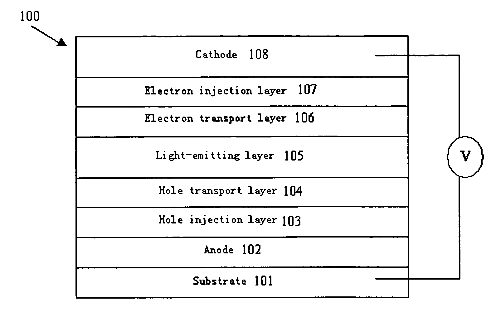
[0052](1) Device structure:

[0053]ITO / MTDATA(30 nm) / NPB(30 nm) / Alq3(55 nm) / Li3N(0.8 nm) / AI(150 nm)

[0054](2) Preparation of an organic layer:

[0055]The preprocessed glass substrate is placed in a vacuum chamber which is pumped to 1×10⁻³ Pa. A MTDATA film of 30 nm is evaporated at an evaporation rate of 0.1 nm / s. Then, a layer of hole transport material NPB of 30 nm is evaporated on above film at an evaporation rate of 0.1 nm / s. On the hole transport layer, Alq3 of 55 nm is evaporated for a light-emitting layer and an electron transport layer of the device.

[0056]Wherein the glass substrate is comprised of an ITO (Indium Tin Oxide) film and a substrate. The Sheet Resistance of the ITO film is 50Ω, and its thickness is 150 nm.

[0057](3) Preparation of an electron injection layer:

[0058]After evaporating the electron transport layer, Li3N of 0.8 nm is evaporated at an evaporation rate of 0.008 nm / s under temperature of 350° C. for an electron injection layer of the device.

[0059](4) Preparati...

embodiment 2

[0062](1) Device structure:

[0063]ITO / MTDATA(30 nm) / NPB(30 nm) / Alq3(55 nm) / K3N(1.5 nm) / Al(150 nm)

[0064](2) Preparation steps are the same with Embodiment 1 except after evaporating the electron transport layer, K3N of 1.5 nm is evaporated.

embodiment 3

[0065](1) Device structure:

[0066]ITO / MTDATA(30 nm) / NPB(30 nm) / Alq3(55 nm) / Cs3N(2.0 nm) / Al(150 nm)

[0067](2) Preparation steps are the same with Embodiment 1 except after evaporating the electron transport layer, Cs3N of 2.0 nm is evaporated.


PUM


Abstract

The present invention relates to an organic electroluminescence device comprising a substrate, an anode, a hole injection layer, a hole transport layer, a light-emitting layer, an electron transport layer, an electron injection layer, and a cathode, wherein the electron injection layer contains alkali metal nitride and has a thickness of 0.2-10 nm. The organic electroluminescence device of the present invention has improved electron injection from the cathode to the organic layer, high device luminance and efficiency, long device lifetime, low material poisonousness, wide choice of film-forming thickness and low film-forming temperature.

Description

RELATED APPLICATIONS[0001]This application claims priority under 35 USC §119 to Chinese patent applications 2005 / 10064538.X filed Apr. 13, 2005 and 2005 / 10117296.6 filed Nov. 4, 2005.TECHNICAL FIELD OF THE INVENTION[0002]The present invention relates to an organic electroluminescence device, and more particularly, to an organic electroluminescence device with an improved electron injection layer.BACKGROUND OF THE INVENTION[0003]An organic electroluminescence flat display has many significant advantages, such as initiative light-emitting, light, thin, good contrast, independence of an angle, low power consumption and the like. In 1963, an organic electroluminescence device was fabricated by Pope et al with an anthracene single crystal. However, the first high efficient organic light-emitting diode (OLED) fabricated by vacuum evaporation was an OLED developed by C. W. Tang et al in 1987, wherein aniline-TPD was used as a hole transport layer (HTL), and a complex of aluminium and 8-hyd...

Claims


Application Information

Patent Timeline
Patent Type & Authority Patents(United States)
IPC IPC(8): H01L35/24H01L51/00
CPCC09K11/06H01L51/5092H05B33/14C09K2211/1033C09K2211/1037H10K50/171
Inventor QIU, YONGGAO, YUDIZHANG, DEQIANGWANG, LIDUO
Owner TSINGHUA UNIV
Why Eureka
Try Eureka