
Semiconductor device and method for manufacturing the same

a technology of semiconductor substrates and semiconductor layers, applied in the direction of identification means, discharge tubes, luminescnet screens, etc., can solve the problems of affecting the characteristics of transistors, affecting the performance of transistors, and affecting the stability of the device, so as to reduce the localized level density, prevent and reduce the effect of surface contamination

Inactive Publication Date: 2010-09-14
SEMICON ENERGY LAB CO LTD
View PDF10 Cites 14 Cited by
  • Summary
  • Abstract
  • Description
  • Claims
  • Application Information

AI Technical Summary

Benefits of technology

The present invention provides a method for manufacturing semiconductor devices using a glass substrate for cost reduction purposes. However, there are challenges in bonding a single-crystal silicon layer to a glass substrate due to the high temperature required for the conventional heat treatment method. The invention aims to solve this problem by providing a method for manufacturing a semiconductor device with a single-crystal silicon layer over a glass substrate that reduces warping of the glass substrate and improves the bonding strength between the silicon layer and the glass substrate. Additionally, the invention addresses the issue of strain stress and space generation between adjacent sheets caused by processing accuracy of semiconductor substrates and positioning accuracy of sheets. The invention also provides a method for manufacturing a plurality of panels using a single mother glass substrate efficiently by optimizing the size of semiconductor substrates and sheets.

Problems solved by technology

However, in the case of forming an SOI substrate by bonding single-crystal silicon to a glass substrate that is used in a liquid crystal panel or the like for cost reduction of the substrate, there has been a problem in that such heat treatment at a high temperature causes warpage of the glass substrate.
In addition, there is also a problem in that strain stress is applied to the single-crystal silicon layer and characteristics of the transistor are adversely affected.
In other words, even when a single-crystal silicon layer is disposed over a glass substrate and a transistor is manufactured using the single-crystal silicon layer, sufficient characteristics cannot be obtained with a conventional technique.

Method used


Image

  • Semiconductor device and method for manufacturing the same
  • Semiconductor device and method for manufacturing the same
  • Semiconductor device and method for manufacturing the same

Examples


embodiment mode 1

[0063]First, a top view of a semiconductor substrate 200 which has a thin circular shape is shown in FIG. 3A. As is shown in FIG. 3A, the semiconductor substrate 200 has a flat as a part of its rim to indicate crystallographic orientation. Here, a 5-inch silicon wafer (125 mm in diameter) is used as an example. Note that an 8-inch silicon wafer (200 mm in diameter) or a 12-inch silicon wafer (300 mm in diameter) can be used if needed.

[0064]A silicon oxynitride layer 201 is formed over the semiconductor substrate 200. A thickness of the silicon oxynitride layer 201 may be set as appropriate by a practitioner and may be 10 to 500 nm (preferably 10 to 150 nm). The silicon oxynitride layer 201 later serves as a part of an insulating layer in an SOI substrate. Note that the silicon oxynitride layer 201 can be formed by a method such as a CVD method like a plasma CVD method or a low pressure CVD method, or a sputtering method. For example, the silicon oxynitride layer 201 can be formed ov...

embodiment mode 2

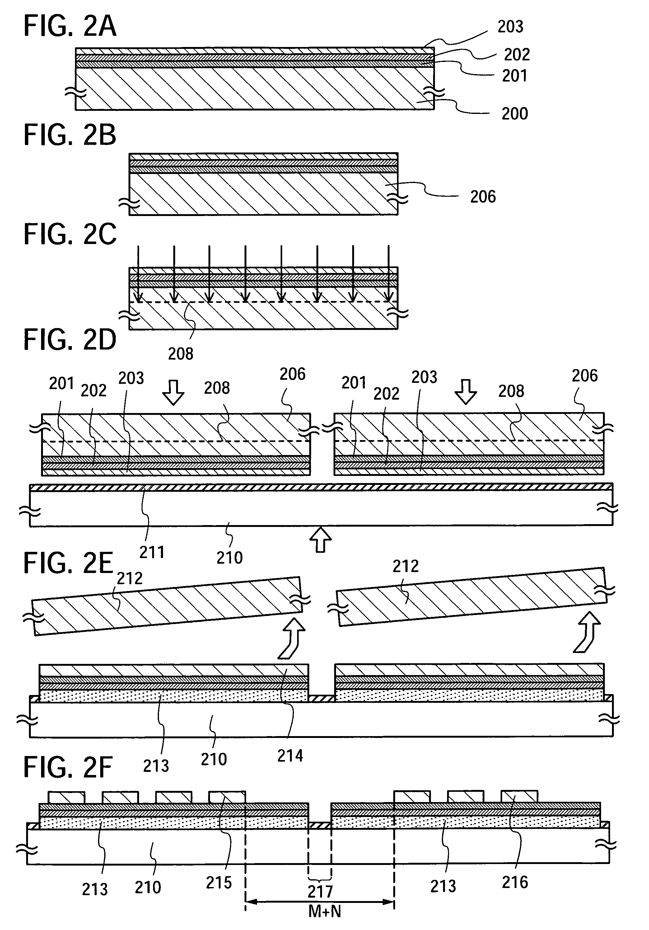
[0151]This embodiment mode describes a method for manufacturing an SOI substrate which includes steps different from the steps in FIGS. 2A to 2F below.

[0152]In FIG. 6A, a p-type or an n-type single crystal silicon substrate (silicon wafer) is typically used as a semiconductor substrate 400.

[0153]Then, the semiconductor substrate 400 is ground or cut so as to be a rectangle sheet 406.

[0154]Then, degreasing washing is performed on the sheet 406 and an oxide film on the surface is removed and thermal oxidation is performed. As thermal oxidation, normal dry oxidation may be performed; however, oxidation in an oxidation atmosphere in which a halogen is added is preferably performed. For example, thermal treatment is performed at a temperature of equal to or higher than 700° C. in an atmosphere containing HCl at 0.5 to 10 volume % (preferably 3 volume %) with respect to oxygen. Preferably, thermal oxidation may be performed at a temperature of 950 to 1100° C. The processing time may be 0....

embodiment mode 3

[0177]This embodiment mode describes an example in which a semiconductor device is manufactured using a plurality of single-crystal semiconductor layers which are disposed over a support substrate, which are manufactured according to Embodiment Mode 1 or Embodiment mode 2.

[0178]A semiconductor device having a light emitting element can be formed according to the present invention, and the light emitting element emits light by any one of bottom emission, top emission, or dual emission. This embodiment mode describes an example of a method for manufacturing a semiconductor device with high yield, in which a semiconductor device having a display function (also referred to as a display device or a light emitting device) is manufactured as a bottom-emission, dual-emission, or top-emission semiconductor device with high performance and high reliability, with reference to FIGS. 7A, 7B, and 8.

[0179]First, island-shaped single-crystal semiconductor layers are formed over a support substrate ...


PUM

PropertyMeasurementUnit
temperatureaaaaaaaaaa
sizeaaaaaaaaaa
sizeaaaaaaaaaa

Abstract

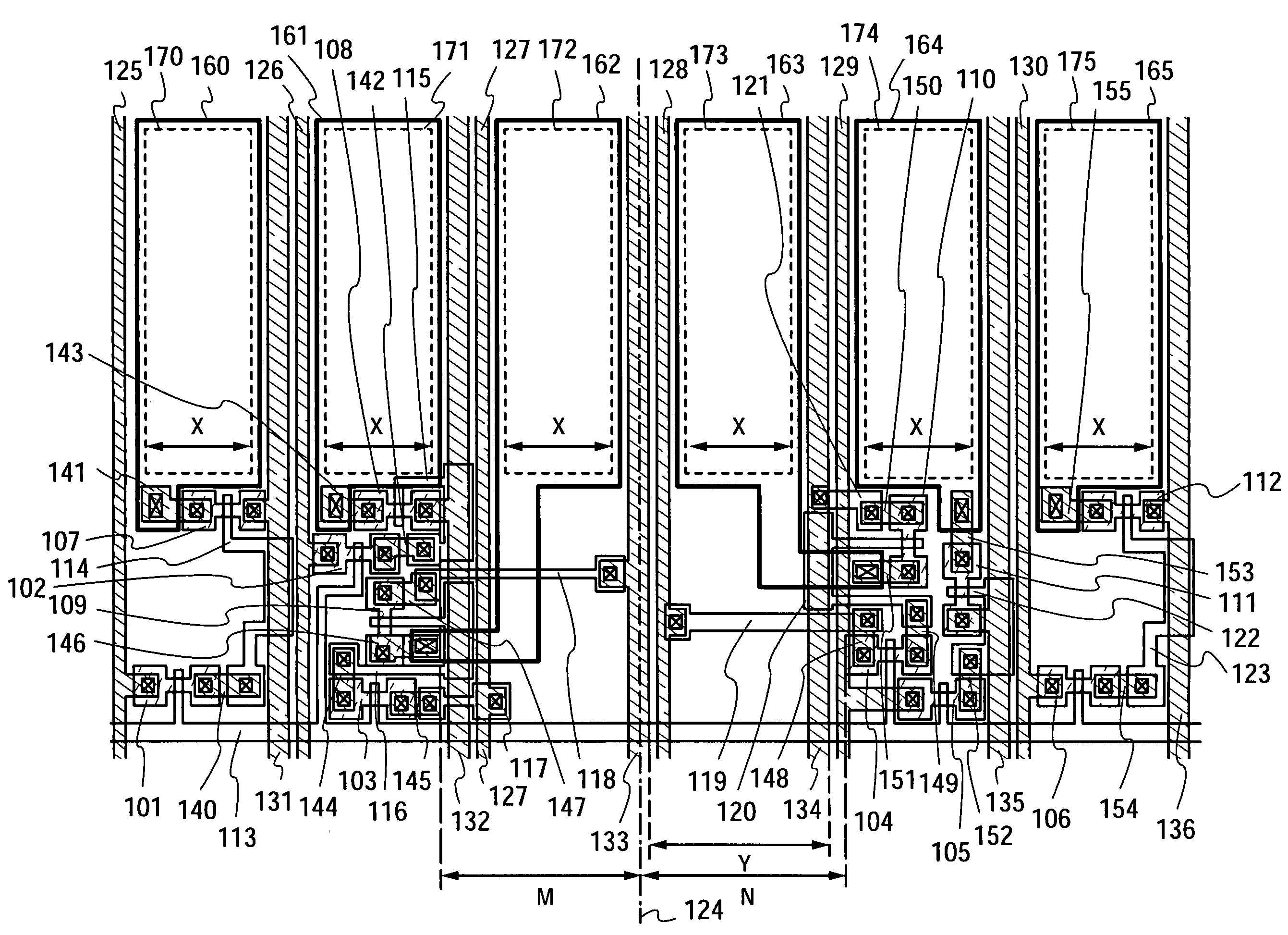
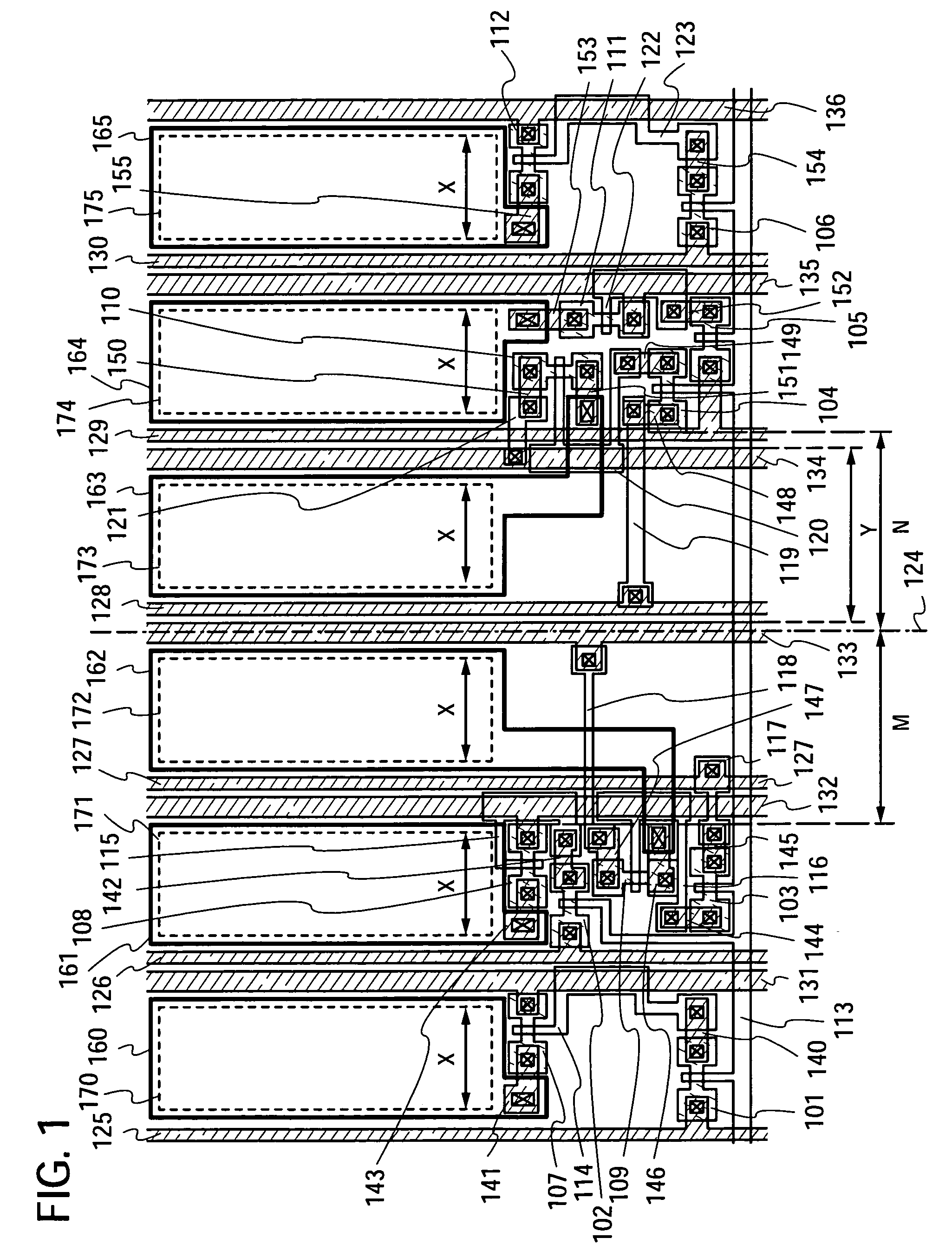
A plurality of rectangle semiconductor substrates are attached to a single mother glass substrate. A pixel structure is determined so that even if a gap or a an overlapping portion is generated in a boundary between a plurality of semiconductor substrates, a single-crystal semiconductor layer does not overlap with the gap or the overlapping portion. Two TFTs are located in a first unit cell including the first light emitting element, four TFTs are located in a second unit cell including the second light emitting element, and no TFT is located in a third unit cell including the third light emitting element. A boundary line is between the third unit cell and a fourth unit cell.

Description

TECHNICAL FIELD[0001]The present invention relates to semiconductor devices which have circuits including thin film transistors (hereinafter, referred to as TFTs), and a method for manufacturing the semiconductor devices. For example, the present invention relates to electro-optical devices typified by liquid crystal display panels, or electronic appliances which have light emitting display devices including an organic light emitting element as a component.[0002]Note that a semiconductor device refers to any device which can function by utilizing semiconductor characteristics in this specification. Electro-optical devices, semiconductor circuits, and electronic appliances are all semiconductor devices.BACKGROUND ART[0003]In recent years, attention has focused on a technique for making a thin film transistor (TFT) by using a semiconductor thin film (having a thickness of approximately several to several hundreds of nanometers) formed over a substrate having an insulating surface. The...

Claims


Application Information

Patent Timeline
Patent Type & Authority Patents(United States)
IPC IPC(8): H01L33/00G02F1/1343G02F1/1368G09F9/30G09F9/40H01L21/02H01L21/265H01L21/322H01L21/336H01L27/12H01L29/786H01L51/50H05B33/10H05B33/12H05B33/14
CPCH01L27/1214H01L27/1266H01L27/3244H10K59/12H01L21/76254
Inventor YAMAZAKI, SHUNPEI
Owner SEMICON ENERGY LAB CO LTD
Learn More