Cluster ion implantation for defect engineering

a technology of defect engineering and cluster ion, which is applied in the direction of basic electric elements, electrical equipment, electric discharge tubes, etc., can solve the problems of crystal damage, electron energy loss, energy (velocity), etc., and achieve the effect of reducing leakage current, reducing defects in the crystalline structure, and improving the performance of the semiconductor junction

Inactive Publication Date: 2011-04-05
SEMEQUIP
View PDF32 Cites 25 Cited by
  • Summary
  • Abstract
  • Description
  • Claims
  • Application Information

AI Technical Summary

Benefits of technology

[0025]Briefly, the present invention to a method of semiconductor manufacturing in which doping is accomplished by the implantation of ion beams formed from ionized molecules, and more particularly to a method in which molecular and cluster dopant ions are implanted into a substrate with and without a co-implant of non-dopant cluster ion, such as a carbon cluster ion, wherein the dopant ion is implanted into the amorphous layer created by the co-implant in order to reduce defects in the crystalline structure, thus reducing the leakage current and improving performance of the semiconductor junctions. Dopant ion compounds of the form AnHx+ and AnRzHx+ are used in order to minimize crystal defects as a result of ion implantation. These compounds include co-implants of carbon clusters with implants of monomer or cluster dopants or simply implanting cluster dopants. In particular, the invention described herein consists of a method of implanting semiconductor wafers implanting semiconductor wafers with carbon clusters followed by implants of boron, phosphorus, or arsenic, or followed with implants of dopant clusters of boron, phosphorus, or arsenic. The molecular cluster ions have the chemical form AnHx+ or AnRzHx+, where A designates the dopant or the carbon atoms, n and x are integers with n greater than or equal to 4, and x greater than or equal to 0, and R is a molecule which contains atoms which, when implanted, are not injurious to the implantation process (for example, Si, Ge, F, H or C). These ions are produced from chemical compounds of the form AbLzHm, where the chemical formula of Lz contains R, and b may be a different integer from n and m may be an integer different from x and z is an integer greater than or equal to zero.
[0029]In a preferred embodiment, the carbon cluster implant is chosen such that the amorphous layer it creates is at least as thick as the end of range of the subsequent dopant implant, so that virtually all of the defects associated with the dopant implant are created in amorphous material. This insures that these defects will be easily annealed out during the subsequent activation step.
[0031]Another alternate embodiment of the invention is to provide a method of manufacturing a semiconductor device, this method being capable of forming ultra-shallow impurity-doped regions of N and P-type conductivity in an auto-amorphized zone, using ionized clusters of the form AnCmHx+, or AnCmRzHx+, where A is a dopant atom such as B, P, or As, n, x and z are integers with 1≦n, 0≦m, and x and z≧0, R is a molecule, radical or ligand which contain atoms that are not injurious to the implantation process or semiconductor device performance, thus limiting the dopant diffusion and eliminating end-of-range defects with a single implant, and furthermore to do so with high productivity. In this preferred embodiment, the carbon cluster implant is chosen such that the amorphous layer it creates is at least as thick as the end of range of the subsequent dopant implant, so that virtually all of the defects associated with the dopant implant are created in amorphous material. This insures that these defects will be easily annealed out during the subsequent activation step. To effectively control diffusion the peak concentration of carbon must be in the range of 1E17 to 1E19 carbon / cm3.
[0032]The present invention increases the benefits of N-type cluster implantation, for example, by using significantly larger dopant clusters, such as, phosphorus or arsenic clusters having more than 3 dopant atoms. Carbon cluster ions, CxHy+, can be used to deliver low energy high dose carbon ion beam to the semiconductor surface to pre-amorphize the silicon to eliminate channeling and at the same time position C atoms below the surface to substantially reduce B diffusion in the B implant that will immediately follow the C implant. Additionally the carbon cluster exhibits the same charge reducing benefits as the doping clusters.

Problems solved by technology

Damage to the crystal is caused by two energy loss mechanisms that reduce the energy (velocity) of the ions.
Firstly there is electron energy loss where energy form the ion is transferred to the electrons in the material.
This can cause point defects in the crystal.
These defects are easily healed by thermal treatment of a few hundred degrees C. Secondly there is nuclear energy loss that occurs when the ion has a collision with a lattice atom.
This results in momentum transfer to the lattice atom and can actually knock it out of place and give it a velocity which interns strikes another atom causing it to move.
This cascade of displaced atoms can lead to extended defects.
These defects are much more difficult to heal and require higher temperature treatments.
Therefore near the surface where the energy of the ion beam is higher, most of the defects are point defects, but deeper into the material where the energy has been reduced the defects are primarily due to nuclear collisions and are more difficult to anneal out.
The defects at the end of the ion path are call end-of-range defects and are particularly difficult to anneal.
Such high temperature anneals are known to be detrimental to device structures because they cause long diffusion lengths which result in deeper dopant profiles than desired.
Due to the aggressive scaling of junction depths in CMOS processing, the ion energy required for many critical implants has decreased to the point that conventional ion implantation systems cannot maintain the desired wafer throughput.
The limitations of conventional ion implantation systems at low beam energy are most evident in the extraction of ions from the ion source, and their subsequent transport through the implanter's beam line.
Similar constraints affect the transport of the low-energy beam after extraction.
In addition, since the electrostatic forces between ions are inversely proportional to the square of the distance between them, electrostatic repulsion is much stronger at low energy, resulting in increased dispersion of the ion beam.
This phenomenon is called “beam blow-up” and is the principal cause of beam loss in low-energy transport.
In particular, severe extraction and transport difficulties exist for light ions, such as the N-type dopants phosphorus and arsenic.
The use of Ge or Si pre-amorphization implants has been shown to create end-of-range defects which result in increased leakage currents in the fabricated devices.
A detriment to this process is the implanting of fluorine atoms into the semiconductor substrate along with the boron.
This is an undesirable feature of this technique since fluorine has been known to exhibit adverse effects on the semiconductor device.
While this approach produces shallower junctions with good activation, it makes the recovering of implant damage more difficult.
In particular, the end-of-range (EOR) defects created by the widely used Ge pre-amorphization (PAI) implant typically survive low thermal budget treatments, resulting in higher junction leakage.
Leakage current results from defects in the crystalline structure of the substrate caused by the implantation of the dopant.
Although there have been efforts to reduce the defects and thus reduce leakage current in semiconductor junctions, leakage currents in available semiconductors are still at unacceptable levels.

Method used


Image

  • Cluster ion implantation for defect engineering
  • Cluster ion implantation for defect engineering
  • Cluster ion implantation for defect engineering

Examples


Embodiment Construction

Cluster Ion Technology

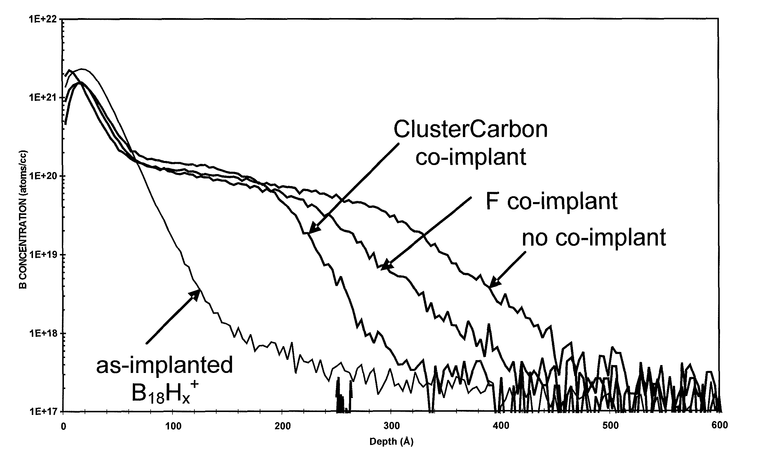
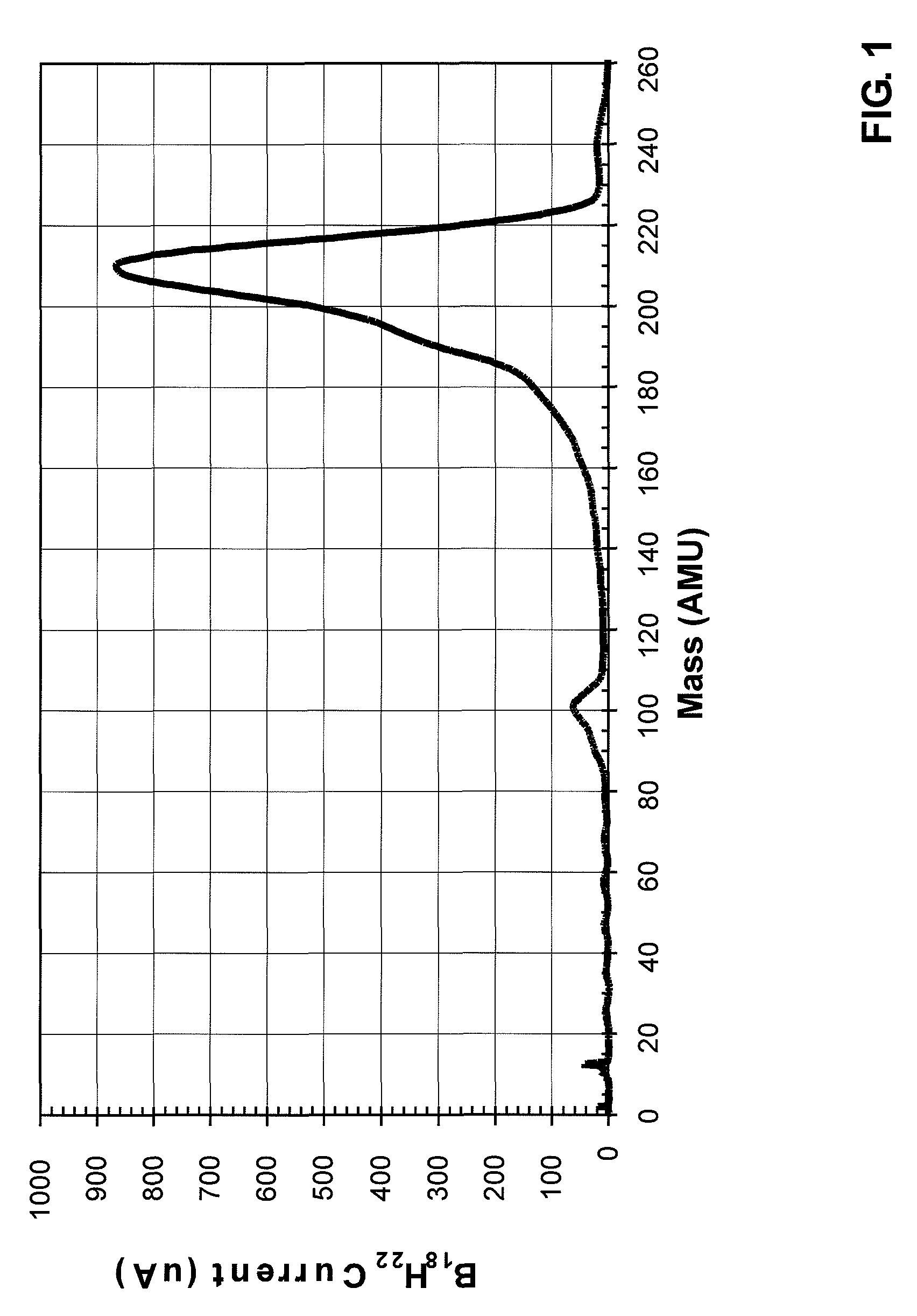
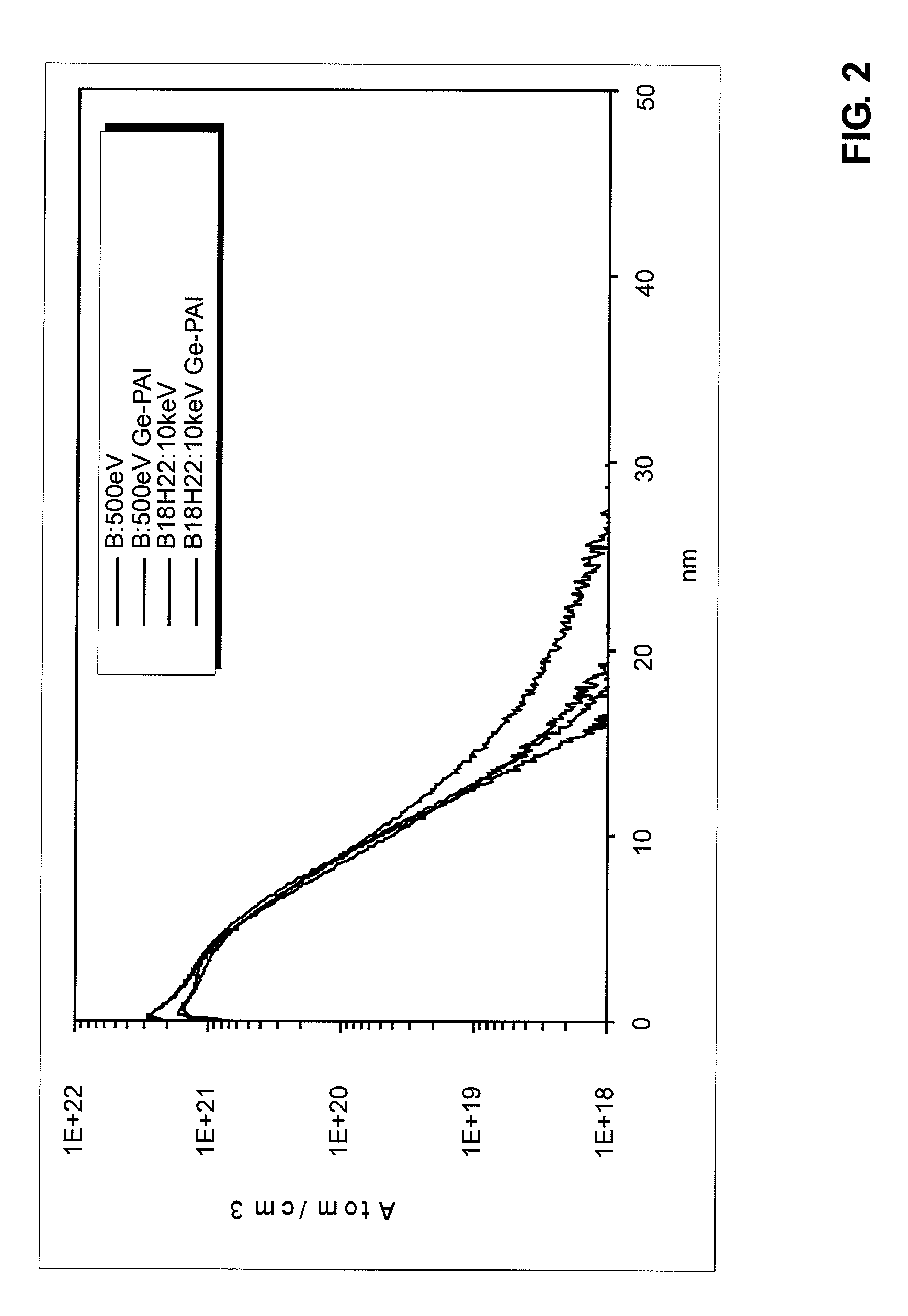
[0074]The present invention to a method of semiconductor manufacturing in which doping is accomplished by the implantation of ion beams formed from ionized molecules, and more particularly to a method in which molecular and cluster dopant ions are implanted into a substrate with and without a co-implant of non-dopant cluster ion, such as a carbon cluster ion, wherein the dopant ion is implanted into the amorphous layer created by the co-implant in order to reduce defects in the crystalline structure, thus reducing the leakage current and improving performance of the semiconductor junctions. In particular, a new implant technology has been developed as an alternative for low energy boron implant. The concept of this technology is to use a molecular ion which contains many boron atoms to avoid the fundamental issues with conventional ion implantation of low energy boron. A new chemical, octadecaborane B18H22, may used as the source of this molecule, boron cluster...


PUM


Abstract

A method of semiconductor manufacturing is disclosed in which doping is accomplished by the implantation of ion beams formed from ionized molecules, and more particularly to a method in which molecular and cluster dopant ions are implanted into a substrate with and without a co-implant of non-dopant cluster ion, such as a carbon cluster ion, wherein the dopant ion is implanted into the amorphous layer created by the co-implant in order to reduce defects in the crystalline structure, thus reducing the leakage current and improving performance of the semiconductor junctions. These compounds include co-implants of carbon clusters with implants of monomer or cluster dopants or simply implanting cluster dopants. In particular, the invention described herein consists of a method of implanting semiconductor wafers implanting semiconductor wafers with carbon clusters followed by implants of boron, phosphorus, or arsenic, or followed with implants of dopant clusters of boron, phosphorus, or arsenic.

Description

CROSS REFERENCE TO RELATED APPLICATIONS[0001]This application is a continuation-in-part of commonly owned U.S. patent application Ser. No. 11 / 634,565, filed Dec. 6, 2006, entitled “System and Method for the Manufacture of Semiconductor Devices by the Implantation of Carbon Clusters” by Wade A. Krull and Thomas N. Horsky, now U.S. Pat. No. 7,666,771, hereby incorporated by reference.BACKGROUND OF THE INVENTION[0002]1. Field of the Invention[0003]The present invention relates to a method of semiconductor manufacturing in which doping is accomplished by the implantation of ion beams formed from ionized molecules, and more particularly to a method in which molecular and cluster dopant ions are implanted into a substrate with and without a co-implant of non-dopant cluster ion, such as a carbon cluster ion, wherein the dopant ion is implanted into the amorphous layer created by the co-implant in order to reduce defects in the crystalline structure, thus reducing the leakage current and im...

Claims


Application Information

Patent Timeline
Patent Type & Authority Patents(United States)
IPC IPC(8): H01L21/265
CPCH01J37/3171H01L21/26506H01L21/823842H01L21/2658H01L21/823814H01L21/26513H01L21/26566
Inventor JACOBSON, DALE C.HORSKY, THOMAS N.KRULL, WADE A.SEKAR, KARUPPANAN
Owner SEMEQUIP
Why Eureka
Try Eureka