Carbon nanotube-based glucose sensor
a glucose sensor and carbon nanotube technology, applied in the direction of optical radiation measurement, diaphragm, immobilised enzymes, etc., can solve the problems of limited potential utility, limited utility of functionalized swnts, and failure to report electrical characteristics of functionalized swnts
- Summary
- Abstract
- Description
- Claims
- Application Information
AI Technical Summary
Benefits of technology
Problems solved by technology
Method used
Image
Examples
example 1
Preparation of 2-(9-(2-thioethyl)-1-(methyl-[methyl]amino) methyl)-phenylboronic acid (II)
(2-bromomethyl)phenylboronic anhydride is prepared as follows: As shown in FIGS. 2-3, orthobromotoluene is reacted with magnesium (1.1 equivalents) in diethylether at 25° C. Grignard reagent is added dropwise to a solution of trimethylborate (10 equivalents) in diethylether at −78° C. The mixture is stirred further for 2 hours, then allowed to warm to room temperature, and stirred further for 2 hours. The diethylether is removed under reduced pressure, and the solid recrystallized from water. The product phenylboronic acid is dried in a vacuum oven overnight to produce phenylboronic anhydride (2).
The phenylboronic anhydride is mixed with NBS (N-bromosuccinimide) (1.1 equivalents) and catalytic AIBN (azoisobutylnitrile) in carbon tetrachloride as a solvent. The mixture is refluxed under radiation by a 200 Watt lamp for 2 hours. The solution is filtered when hot and the solvent removed to yield t...
example 2
The self-assembled monolayer of the compound of formula II on a gold submonolayer on carbon nanotubes is prepared as follows.
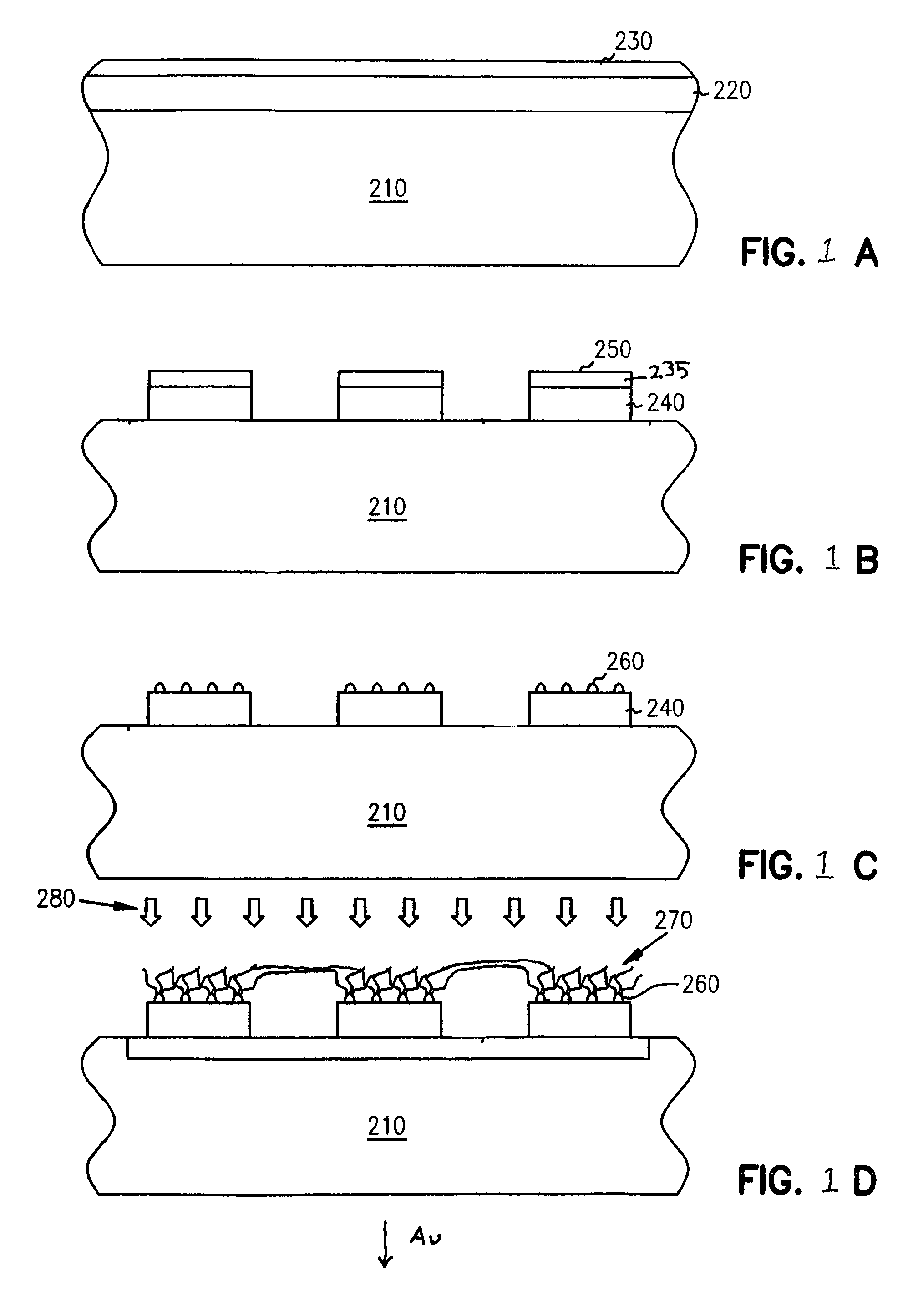
A Superslip® microscope glass coverslip is used as the substrate of the nanotube chip. The coverslip is cleaned in Piranha solution (30% H202:concentrated H2SO4 1:3) for 15 seconds and rinsed carefully with Milli-Q® grade water. The coverslip is then dried in a nitrogen stream and placed in a vacuum evaporator. A platinum film (about 50 nm thickness) is deposited on the coverslip using a Polaron E5000 sputter coating system and a nickel film is deposited onto the platinum film. The sputter coating system is maintained under conditions of 2.0×10⁻² mbar and 20 mA for 180 seconds.
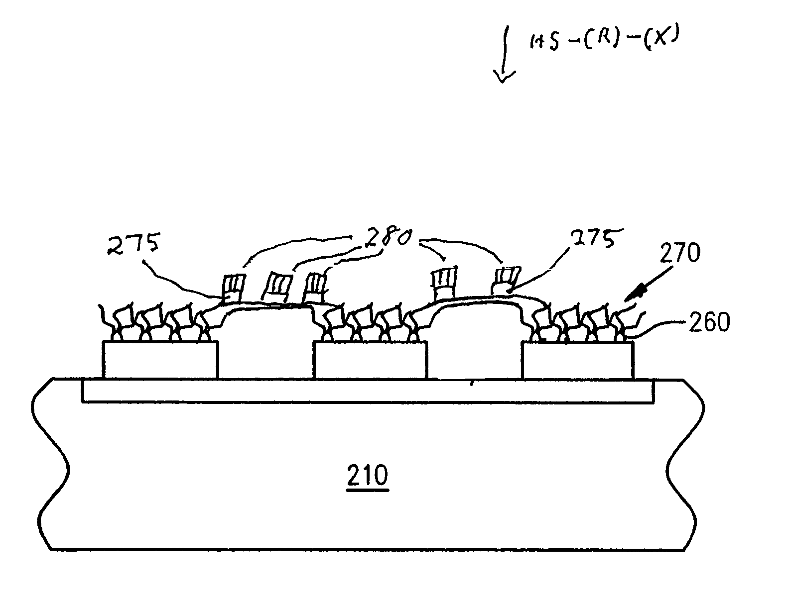
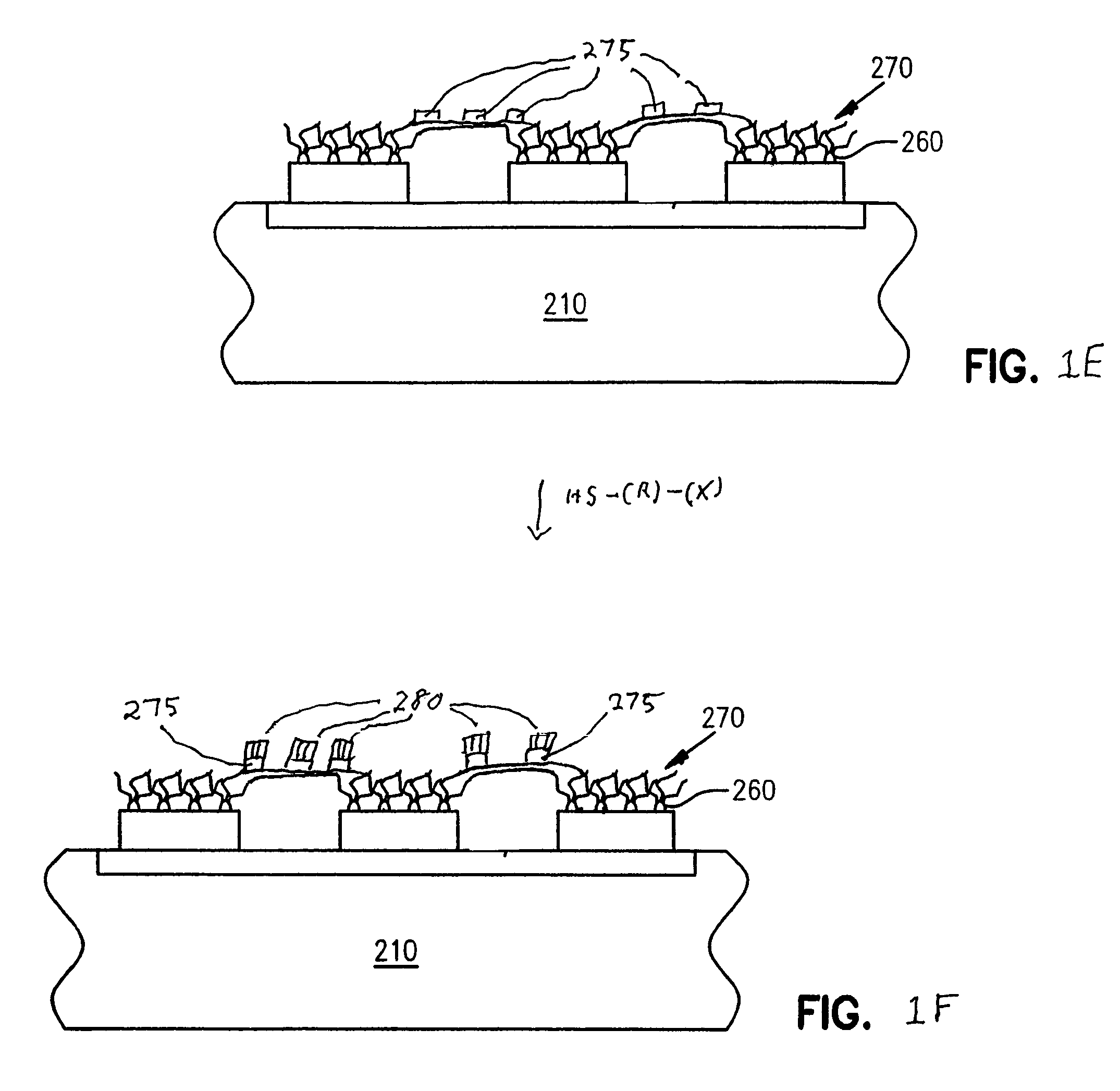
The nickel and platinum films are then patterned to yield an interdigitated finger pattern represented by the islands 250 in FIG. 1B, and the nickel layer is annealed to form islands (260) as shown in FIG. 1D. Carbon nanotubes are then deposited so as to bridge the islands as shown in FI...
PUM
| Property | Measurement | Unit |
|---|---|---|
| conductive properties | aaaaa | aaaaa |
| concentration | aaaaa | aaaaa |
| conductance | aaaaa | aaaaa |
Abstract
Description
Claims
Application Information


