
Method and system for forming copper indium gallium sulfur selenide absorption layer and cadmium sulfide buffer layer under non-vacuum condition

a technology of copper indium gallium sulfur selenide and buffer layer, which is applied in the direction of solid-state diffusion coating, electrolytic capacitor, light-sensitive device, etc., can solve the problems of low material utilization efficiency, low manufacturing cost, and low compactness of the formed cigs absorption layer, so as to improve the lattice match of the primary cigsse layer and improve the photoelectric conversion efficiency and the effect of absorption efficiency

Inactive Publication Date: 2011-08-16
JENN FENG NEW ENERY CO LTD
View PDF2 Cites 10 Cited by
  • Summary
  • Abstract
  • Description
  • Claims
  • Application Information

AI Technical Summary

Benefits of technology

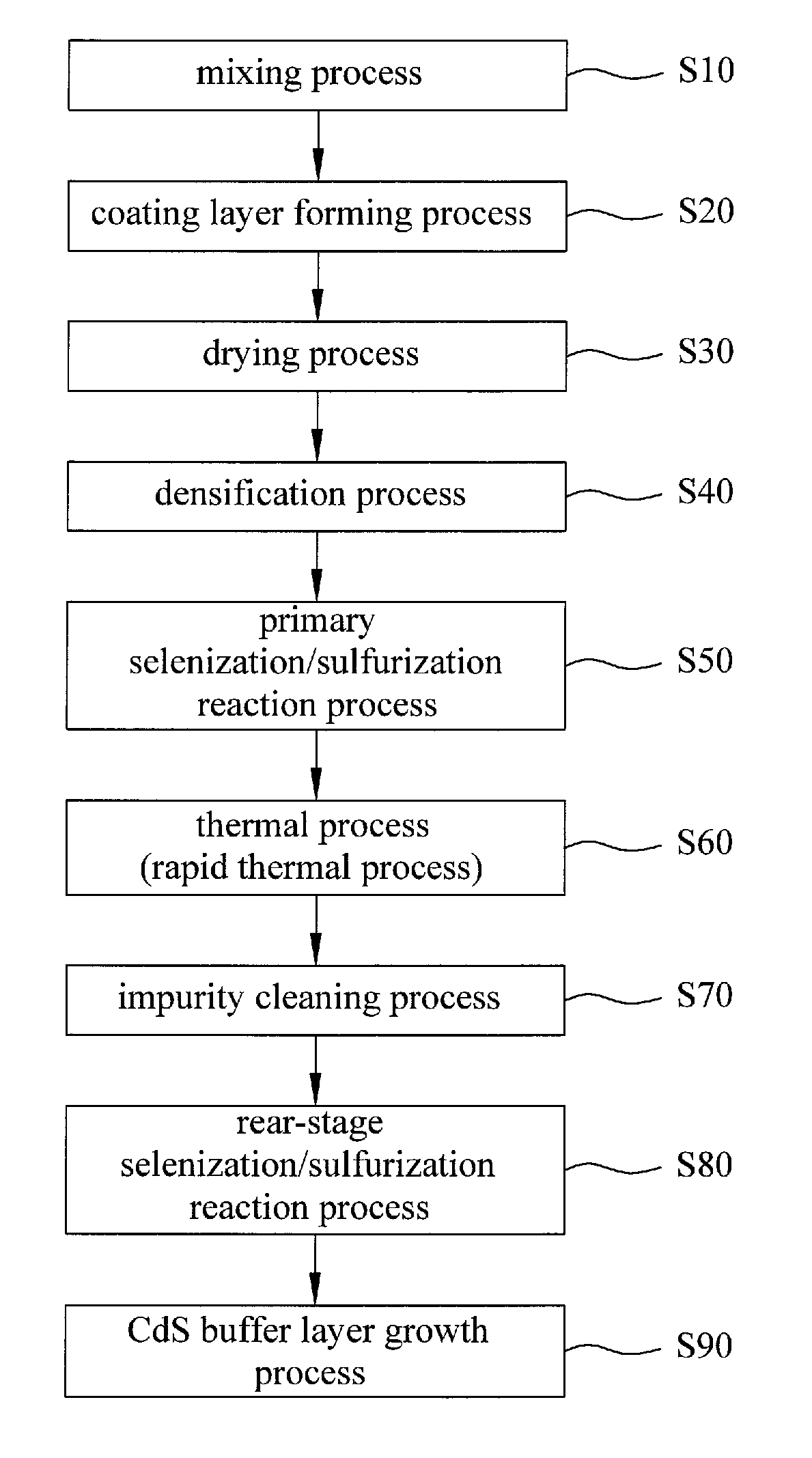
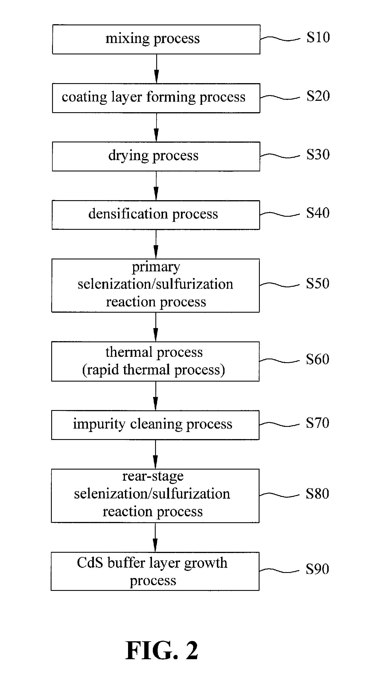
[0010]The main objective of the present invention is to provide a method for forming a copper indium gallium sulfur selenide (CIGSSe) absorption layer and a cadmium sulfide (CdS) buffer layer under non-vacuum condition. In the method of present invention, a coating layer is formed on a back electrode layer on the substrate by mixing slurry and coating it on the back electrode layer. After the substrate is dried, the densification process is carried out using a densification device. Then, a primary sulfurization process and a primary selenization process are carried out to form a primary CIGSSe layer. After that, a thermal process is performed to improve the lattice match of the primary CIGSSe layer. An impurity cleaning process is then performed by using potassium cyanide or bromide to remove impurities of cuprous selenide and copper sulfide. Then, a rear-stage sulfurization process and a rear-stage selenization process are carried out to generate the required CIGSSe absorption layer. Finally, a CdS buffer layer is formed on the CIGSSe layer by a chemical bath deposition. The CIGSSe absorption layer and the CdS buffer layer can be applied to a CIGS solar cell. The absorption efficiency and the photoelectric conversion efficiency of the absorption layer can be increased, and the lattice match of the buffer layer with the absorption layer can be improved. Furthermore, the p-n junction with high efficiency is formed between the absorption layer and the buffer layer so that the manufacturing cost can be reduced and the performance of the overall CIGS solar cell can be improved.

Problems solved by technology

However, in the vacuum processes, the expensive process equipments are required, the material utilization efficiency is low, and the fabricating cost is high.
However, the compactness of the formed CIGS absorption layer is relatively low so that the quaternary compound with the large particle size is not easily formed.
As a result, many grain boundaries exist in the absorption layer, and when the light falls onto these grain boundaries, it may not be successfully converted into electric energy so that the photovoltaic conversion efficiency becomes low.

Method used


Image

  • Method and system for forming copper indium gallium sulfur selenide absorption layer and cadmium sulfide buffer layer under non-vacuum condition
  • Method and system for forming copper indium gallium sulfur selenide absorption layer and cadmium sulfide buffer layer under non-vacuum condition
  • Method and system for forming copper indium gallium sulfur selenide absorption layer and cadmium sulfide buffer layer under non-vacuum condition

Examples


Embodiment Construction

[0016]Reference will now be made in detail to embodiments of the present invention, examples of which are illustrated in the accompanying drawings.

[0017]Referring to FIG. 2, a flow chart of the method according to the present invention is illustrated. As shown in FIG. 2, the method of the present invention starts at S10. A mixing process is performed under non-vacuum condition. In a mixing process, the copper-indium-gallium-sulfur-selenium powder, the solvent, and the additive are mixed to form a CIGSSe slurry. The copper-indium-gallium-sulfur-selenium powder may include at least one of powders of copper-indium (CuIn) alloy, copper-indium-gallium (CuInGa) compound, copper-indium selenide (CuInSe), copper-indium-gallium selenide (CuInGaSe), copper-indium sulfide (CuInS), and copper-indium-gallium sulfide (CuInGaS). The solvent may include at least one of alcohols and amines. The additive may include at least one of dispersant, adhesive, and leveling agent.

[0018]Then upon entering ste...


PUM

PropertyMeasurementUnit
Temperatureaaaaaaaaaa
Lattice constantaaaaaaaaaa
Adhesivityaaaaaaaaaa

Abstract

A method and a system for forming a copper indium gallium sulfur selenide (CIGSSe) absorption layer and a cadmium sulfide (CdS) buffer layer under non-vacuum condition is disclosed. A coating layer is formed on the back electrode layer on the substrate by mixing the slurry on the back electrode layer, and the coating layer formed on the back electrode layer is densified by a densification device after initially dried, and then a primary selenization / sulfurization reaction process is carried out to form a primary CIGSSe layer, and then a thermal process is carried out to improve the lattice match of the primary CIGSSe layer, and then an impurity cleaning process is carried out by using potassium cyanide or bromide to remove the impurities of cuprous selenide and copper sulfide, and then a rear-stage selenization / sulfurization reaction process is carried out to produce the required rear-stage CIGSSe absorption layer. Finally, a CdS buffer layer is formed on the CIGSSe absorption layer by a chemical bath deposition method.

Description

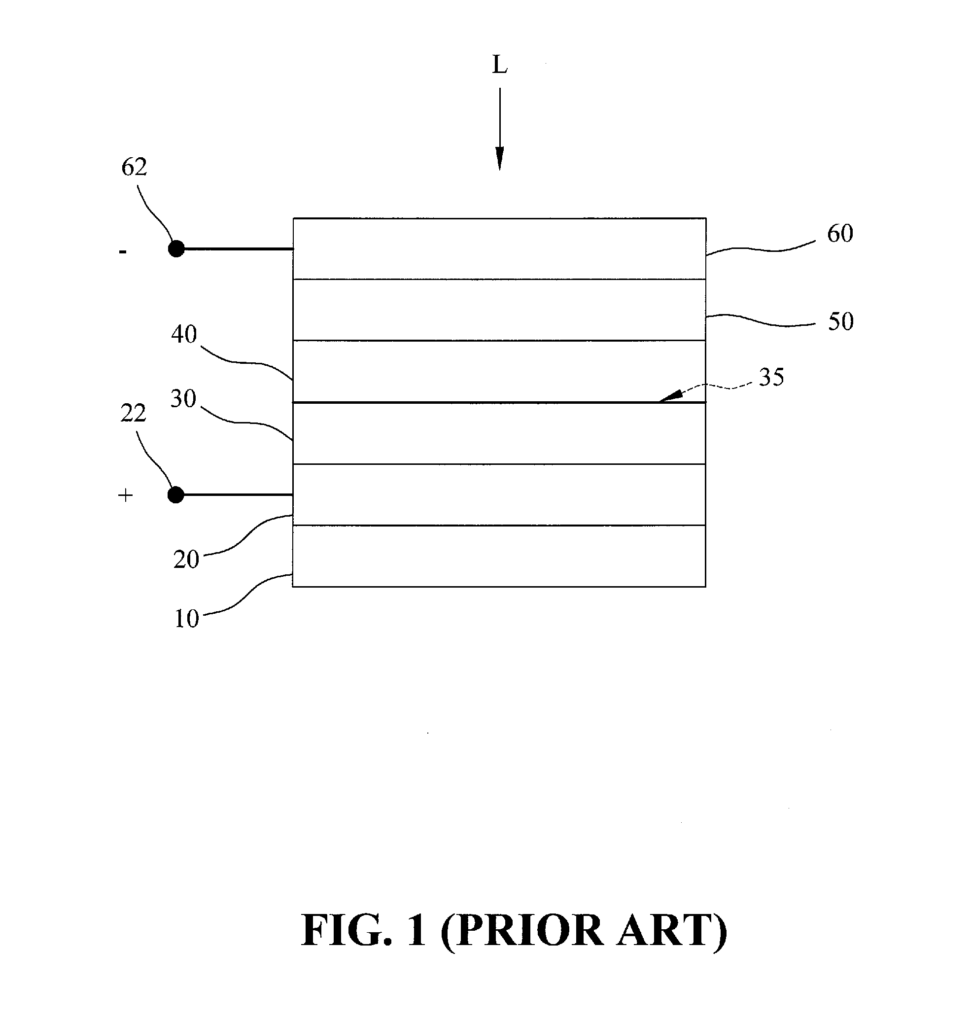
BACKGROUND OF THE INVENTION[0001]1. Field of the Invention[0002]The present invention relates to a method and a system for forming a copper indium gallium sulfur selenide absorption layer and a cadmium sulfide buffer layer, and more specifically to a method and a system which carry out a two-step selenization / sulfurization reaction under non-vacuum condition to form an absorption layer of good quality.[0003]2. The Prior Arts[0004]Due to a rising global trend in green energy, the copper indium gallium diselenide (CIGS) solar cell, which is a complex quaternary alloy, has been studied and developed as a potential energy source in industry. The CIGS solar cell is not restricted by the raw materials, and can be manufactured on a large-area flexible substrate. The conversion efficiency per unit solar cell is up to 20%, and the conversion efficiency of a solar cell module is also up to 14%.[0005]Referring to FIG. 1, a conventional CIGS solar cell is illustrated. As shown in FIG. 1, a CIGS...

Claims


Application Information

Patent Timeline
IPC IPC(8): H01L21/00H01G9/20H01L21/16
CPCC23C8/02C23C10/60C23C26/00H01L31/0322H01L31/0749H01L31/18Y02E10/541
Inventor CHUANG, CHUAN-LUNG
Owner JENN FENG NEW ENERY CO LTD
Learn More