Method and apparatus for processing three-dimensional structure, method for producing three-dimensional shape product and three-dimensional structure

a three-dimensional structure and apparatus technology, applied in the direction of manufacturing tools, optical beam sources, instruments, etc., can solve the problems of difficult to uniformly apply resists to substrates, difficulties and drawbacks of the above-mentioned conventional laser process methods, and the lik

Inactive Publication Date: 2011-11-01
RICOH KK +1
View PDF33 Cites 10 Cited by
  • Summary
  • Abstract
  • Description
  • Claims
  • Application Information

AI Technical Summary

Benefits of technology

[0039]In an eighteenth aspect of the present invention regarding the apparatus for processing a three-dimensional structure according to the sixteenth aspect, the mask means allows the transmission pattern of the process laser light to be varied, and the process laser light can be irradiated several times onto the same portion after changing the transmission pattern.

Problems solved by technology

The etching method in the conventional photolithography requires a number of complicated processes, such as resist application, exposure, development, baking and so on.
In the case of a three-dimensional process where the depth is altered in accordance with the position, the shape has to be controlled using a number of expensive masks.
Moreover, it is very difficult to uniformly apply a resist to a substrate due to the surface roughness, when it is partially processed in a three dimension.
However, there are difficulties and drawbacks in the above-mentioned conventional laser process methods.
For instance, the process using the CO2 or YAG laser is fundamentally based on the thermal process, so that it is difficult to process a polymer, low melting material or the like in a high precision, because the material to be processed in the vicinity of the area irradiated by the laser light is thermally deformed and / or melted.
In the case of processing metals, thermally disturbed layers in the vicinity of the process area appear due to a high thermal conductivity, so that the deterioration of shape or profile in the area often occurs due to the melting, re-solidification and the like.
Moreover, the application of the process using the excimer laser or the harmonic of the YAG laser is generally restricted to the materials having high absorption efficiency for such a laser wavelength due to the difficulty in the process.
In this laser process, it is also difficult to form the bottom surface of the material to be processed in a uniform height and flatness, and it is usually necessary to precisely control the beam shape of the laser light using an expensive optical system.
Nevertheless, it is difficult to provide a three-dimensional process of the material to be processed having a uniform bottom surface due to the interference with the beams diffracted or split from the mask.
It is particularly difficult to form a flat bottom surface in the precision of the order of several tens nm, which precision is required for producing optical elements.
In this case, an expensive optics for forming a flat bottom surface must be provided, as similarly said abrasion is applied.
In these lasers, the beam transverse mode is normally a single mode, and the beams diffracted in the mask are apt to interfere with each other.
Moreover, there arise problems that the flatness of the processed surface is reduced due to speckle pattern and a fine period generates due to the polarization of the laser light, thereby making it difficult to produce flat surfaces in the material to be processed.
Although the upper thin layer of the material to be processed can also be removed by the thin layer processing method using the conventional laser abrasion, no marked improvement in the surface roughness on the bottom surface of the material to be processed can be obtained, compared with that of the above-mentioned laser abrasion.
In the case of only absorbent material being employed, a deep depth process can hardly be carried out by a one-shot laser radiation.
In case of carrying out a deeper depth process, there is a problem that the quality of the finished material to be processed may be reduced due to the thermal effect.
In the method of removing the upper layer using the absorbent layer of the bottom surface, the process of the absorbent layer also advances, so that it is difficult to control the depth in a three-dimensional manner or it is necessary to control the depth by several times irradiating the laser light.
In any case, it is difficult to control the process of the three-dimensional shape available in an optical device in the precision of order of nano-meter.

Method used


Image

  • Method and apparatus for processing three-dimensional structure, method for producing three-dimensional shape product and three-dimensional structure
  • Method and apparatus for processing three-dimensional structure, method for producing three-dimensional shape product and three-dimensional structure
  • Method and apparatus for processing three-dimensional structure, method for producing three-dimensional shape product and three-dimensional structure

Examples


first embodiment

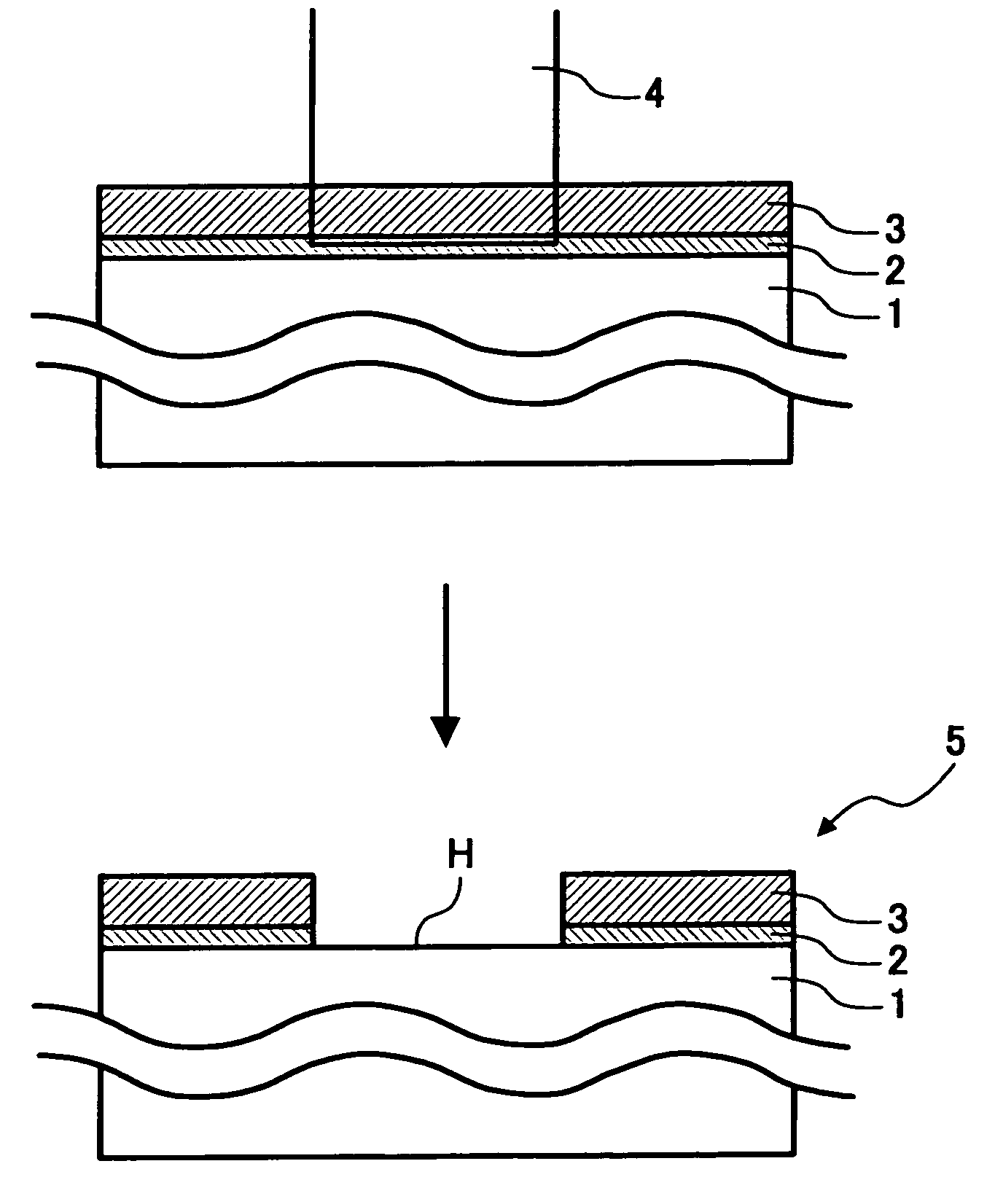
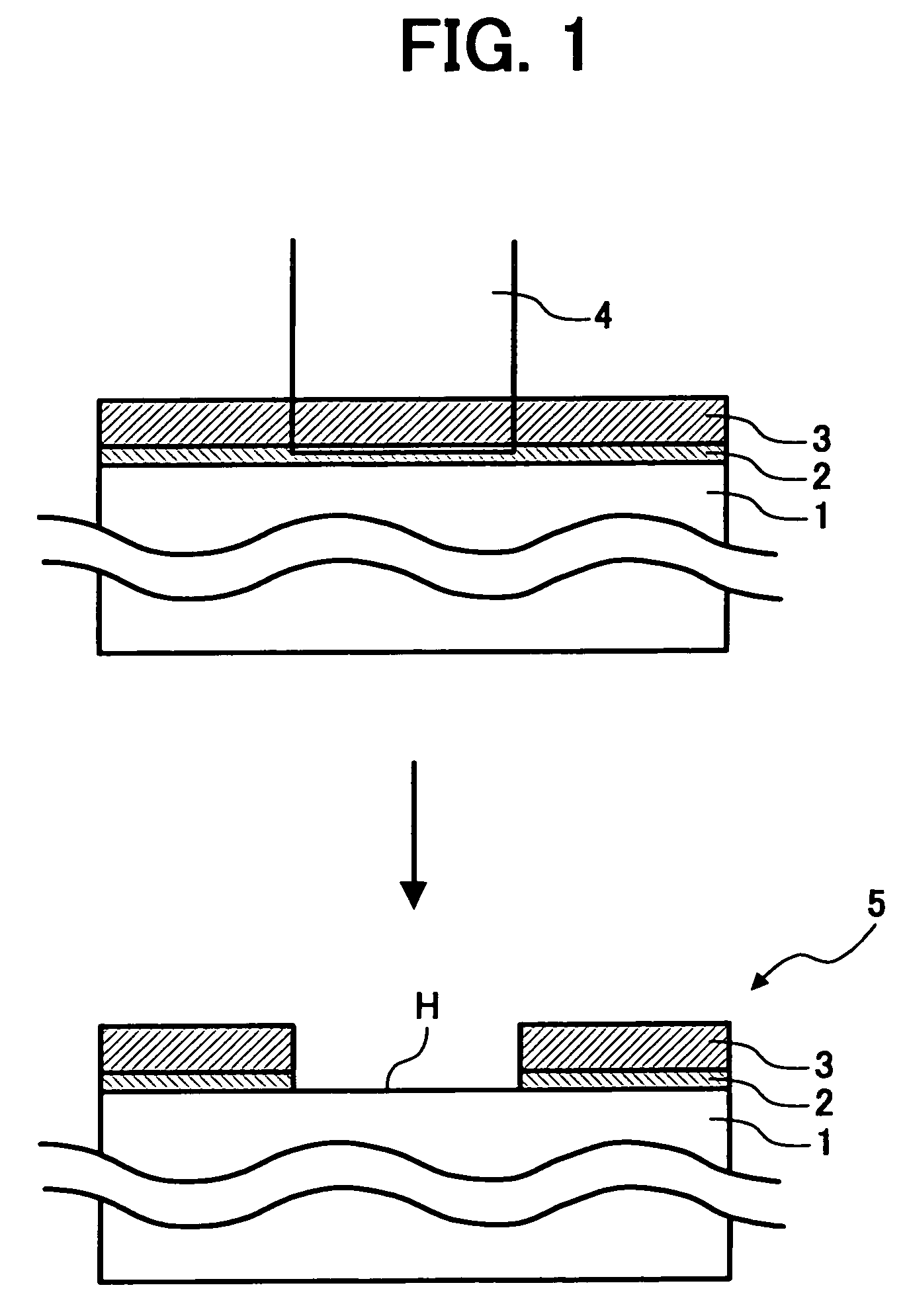
[0072]FIG. 1 is a sectional view of a first embodiment in a method for producing a three-dimensional structure according to the invention.

[0073]As shown in FIG. 1, the three-dimensional structure 5 comprises a flat substrate 1 having a flat and smooth surface of glass, Si, SUS or the like; a thin layer for absorption of laser light 2 deposited onto the flat substrate 1; and a transparent layer 3 capable of transmitting a process laser light 4 towards the thin layer for absorption of laser light 2. In the case of a SUS substrate being used for the flat substrate 1, Al, Cu, Ni or the like may be used as a material for the thin layer for absorption of laser light.

[0074]The three-dimensional structure 5 is provided with a removed material section having a very small size where part of the transparent layer 3 and part of the thin layer for absorption of laser light 2 are removed by the absorption of the process laser light 4 incident from the transparent layer 3 in the thin layer for abs...

example 1

[0087]Referring to FIG. 1, example 1 of the laser processing method in the invention will be described.

[0088]As shown in FIG. 1, a thin layer for absorption of laser light 2 made of Ni or the like is deposited onto a flat substrate 1 made of glass, Si or the like, in this example, a glass substrate having a flat upper surface. A transparent layer 3 made of a light transmitting material, such as acrylic resin, ITO (Indium Tin Oxide) or the like is deposited onto the upper surface of the layer 2. A process laser light 4 having certain intensity is spatial-selectively irradiated onto the material to be processed thus laminated from the upper side of the transparent layer 3.

[0089]The certain intensity of the process laser light 4 implies the intensity where almost all of the energy of the laser light is absorbed in the thin layer for absorption of laser light 2. That is, an injection pulse energy E0 of the process laser light 4 absorbed in the thin layer for absorption of laser light 2 ...

second embodiment

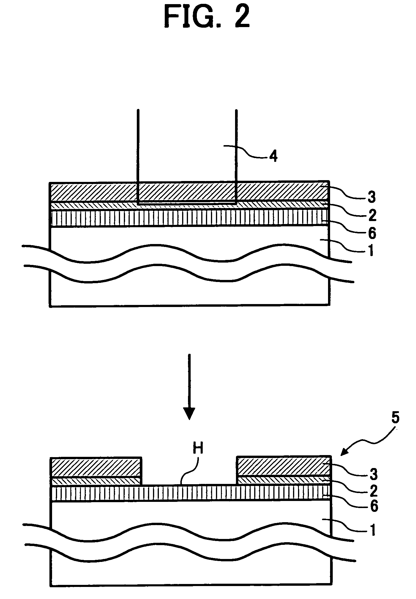
[0092]FIG. 2 is a sectional view of a second embodiment in a method for producing a three-dimensional structure according to the invention.

[0093]As shown in FIG. 2, a three-dimensional structure 5 comprises a flat substrate 1 made of glass, Si, SUS or the like and having a flat surface; a thermal isolation layer 6 deposited on the flat substrate 1; a thin layer for absorption of laser light 2 deposited on the thermal isolation layer 6; and a transparent layer 3 for transmitting a process laser light 4 towards the thin layer for absorption of laser light 2.

[0094]Moreover, the three-dimensional structure 5 in the second embodiment is equipped with a finely removed material section formed by removing part of the transparent layer 3 and part of the thin layer for absorption of laser light 2 due to the absorption of the process laser light 4 incident from the side of the transparent layer 3 in the thin layer for absorption of laser light 2; and an interface on the downstream side of the ...


PUM

PropertyMeasurementUnit
wavelengthaaaaaaaaaa
thicknessaaaaaaaaaa
thicknessaaaaaaaaaa

Abstract

An apparatus for processing a three-dimensional structure having a fine three-dimensional shape and a smooth surface is disclosed in which the three-dimensional structure is usable for an optical device. The process method includes depositing a thin layer for absorption of laser light on a flat substrate; depositing a transparent layer on the thin layer for absorption of laser light; and irradiating a process laser light, passing through the transparent layer; in which pulse injection energy of the process laser light is set to be the same as or smaller than the maximum pulse injection energy capable of exposing a surface of the thin layer in front in the incident direction of the process laser light, and to be set the same as or greater than the minimum pulse injection energy capable of removing the transparent layer in rear in the incident direction of the process laser light.

Description

BACKGROUND OF THE INVENTION[0001]1. Field of the Invention[0002]The present invention relates to a method and an apparatus for processing a three-dimensional structure, a method for producing a product having a three-dimensional shape, and a three-dimensional structure, wherein a fine structure can be formed directly on a material to be processed by irradiating a laser beam, and more specifically to a method and an apparatus for processing a three-dimensional structure, a method for producing a product having a three-dimensional shape, and a three-dimensional structure, wherein a three-dimensional structure with a smooth flat bottom surface can be formed in a high controllability with respect to the process, using one-shot laser light pulses.[0003]In particular, the object of the present invention is to produce in a high precision a product which requires to form a very fine structure, and thereby the present invention relates to a product having a fine three-dimensional shape, in w...

Claims


Application Information

Patent Timeline
Patent Type & Authority Patents(United States)
IPC IPC(8): B23K26/00B23K26/18B23K26/40B29C33/38B29C67/00G02B5/18G11B7/26
CPCB23K26/18B29C67/007G02B5/1857G11B7/125G11B7/261B81C1/00103B81C99/009B23K26/009B23K26/0656Y10T428/24917G03H2001/0478B81C2201/0143B81B2203/033B81B2203/0392Y10S428/913Y10T428/24942Y10T428/12396Y10T428/12389Y10T428/24926B29C33/3857B23K26/066B29C64/129Y10T428/31623
Inventor YAMADA, YASUFUMIMIDORIKAWA, KATSUMIKUMAGAI, HIROSHI
Owner RICOH KK
Why Eureka
Try Eureka