Method for preparing one dimensional spin photonic crystal device and one dimensional spin photonic crystal device prepared by the same

a technology of which is applied in the field of one-dimensional spin photonic crystal devices prepared by the same, can solve the problems of high production cost, long production time, complex process, etc., and achieve the effect of improving the magneto-optical

Inactive Publication Date: 2011-12-06
IUCF HYU (IND UNIV COOP FOUND HANYANG UNIV)
View PDF8 Cites 5 Cited by
  • Summary
  • Abstract
  • Description
  • Claims
  • Application Information

AI Technical Summary

Benefits of technology

Therefore, the present invention has been made in view of the above problems, and it is an object of the present invention to provide a method for preparing a one-dimensional spin photonic crystal device, which is suitable for high integration and industrial-scale production of devices and is economically effective and inexpensive.
It is another object of the present invention to provide a one-dimensional spin photonic crystal device having improved properties, particularly magneto-optical effects.
In accordance with another aspect of the present invention, there is provided a one-dimensional spin photonic crystal having improved magneto-optical effects, comprising a substrate and a thin film deposited on the substrate, wherein the thin film includes magnetic and nonmagnetic regions formed by the interference of laser beams generated from a femtosecond laser light source. The thin film may include Co2MnSi, and the substrate may include glass.

Problems solved by technology

In addition, such conventional methods suffer from various disadvantages such as complexity of processes, long production time, high production costs and therefore consequent lack of economic rationality.

Method used


Image

  • Method for preparing one dimensional spin photonic crystal device and one dimensional spin photonic crystal device prepared by the same
  • Method for preparing one dimensional spin photonic crystal device and one dimensional spin photonic crystal device prepared by the same
  • Method for preparing one dimensional spin photonic crystal device and one dimensional spin photonic crystal device prepared by the same

Examples


example 1

Example 1-1

Thin Film Deposition

An amorphous Co2MnSi thin film was deposited on a glass substrate using magnetron sputtering.

More specifically, a sputtering target was prepared from a Co2MnSi ingot produced by arc melting a stoichiometric mixture of Co, Mn, and Si powders. The sputtering target had a composition of Co(99.5%, SIGMA-ALDRICH):Mn(99.98% SIGMA-ALDRICH):Si(99.95%, SIGMA-ALDRICH) in a ratio of 2:1:1, and a temperature elevation rate was 50□ / min. After preparation of the Co2MnSi ingot was complete, the ingot was ground into powder by wet ball milling and then compressed to prepare a sputtering target having a size of 2 inches.

Thereafter, an amorphous Co2MnSi thin film was deposited on a glass substrate using radio-frequency magnetron sputtering (RF magnetron sputtering) at room temperature under a base pressure of less than 3×10⁻⁷ Torr. The argon pressure was kept at 1 mTorr during deposition, and the deposition rate was 7 nm / min.

example 1-2

Preparation of One-Dimensional Spin Photonic Crystals

Interference of femtosecond laser beams was applied to the amorphous Co2MnSi thin film of Example 1-1 to thereby prepare one-dimensional spin photonic crystals having a repeated structure of magnetic and nonmagnetic regions. The process will be described in more detail with reference to the accompanying drawings.

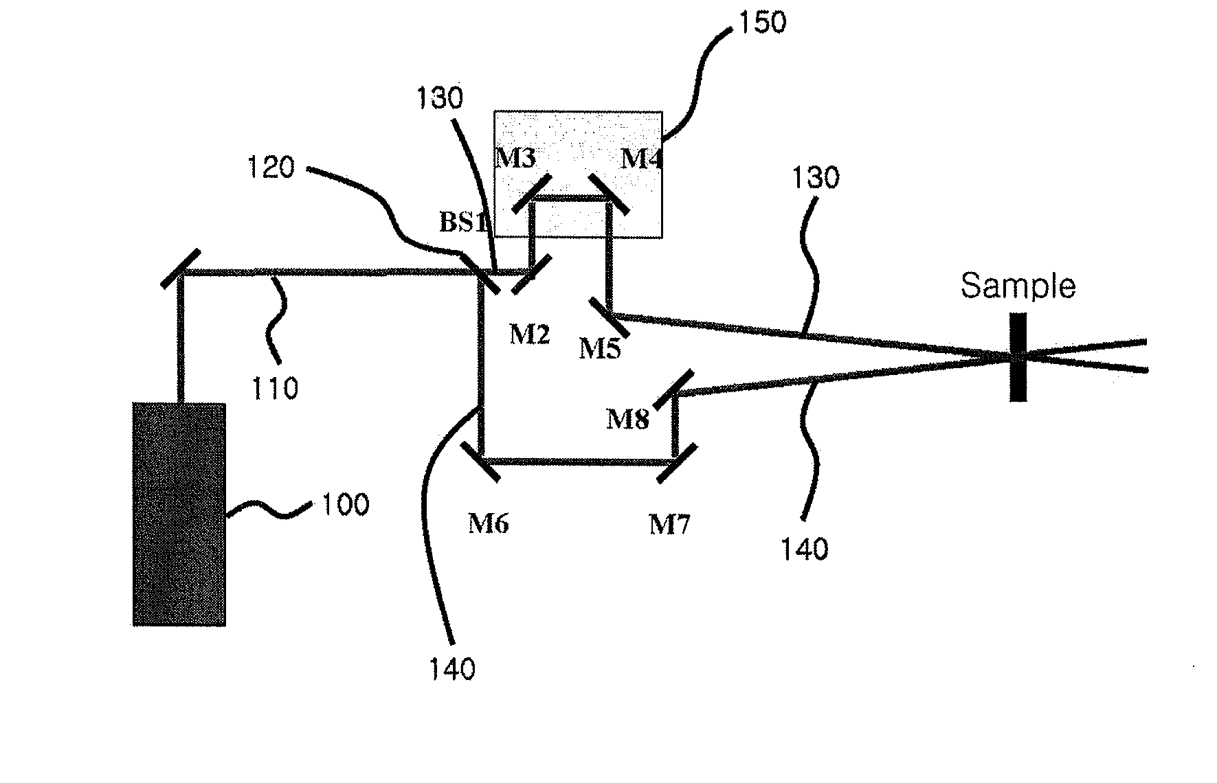
FIG. 1 shows a diagram illustrating the preparation of one-dimensional spin photonic crystals in accordance with one embodiment of the present invention.

Referring to FIG. 1, a femtosecond laser beam 110 generated from a titanium-sapphire laser light source 100 was split into two femtosecond laser beams 130,140 through a beam splitter 120. The first femtosecond laser beam 130 and the second femtosecond laser beam 140 were each incident on a surface of the Co2MnSi thin film via different paths. The femtosecond laser beam 110 had 800 nm output wavelength, 130 fs pulse duration, 1.0 mJ maximum pulse energy, 1 kHz repetition ra...

experimental example 1

Surface Analysis

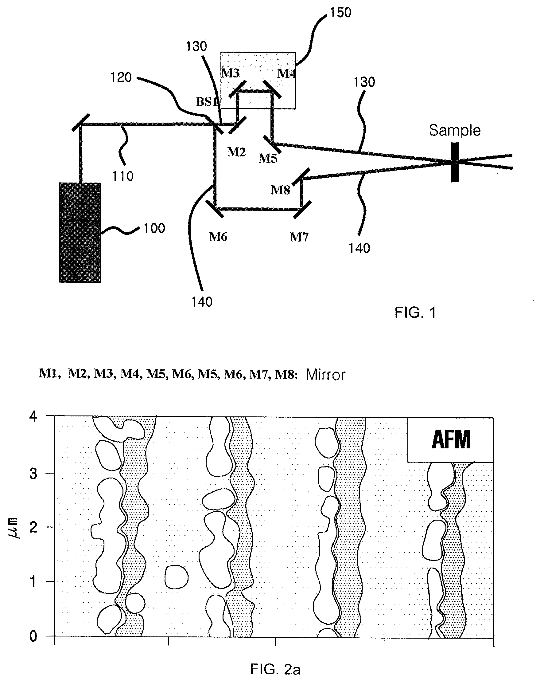
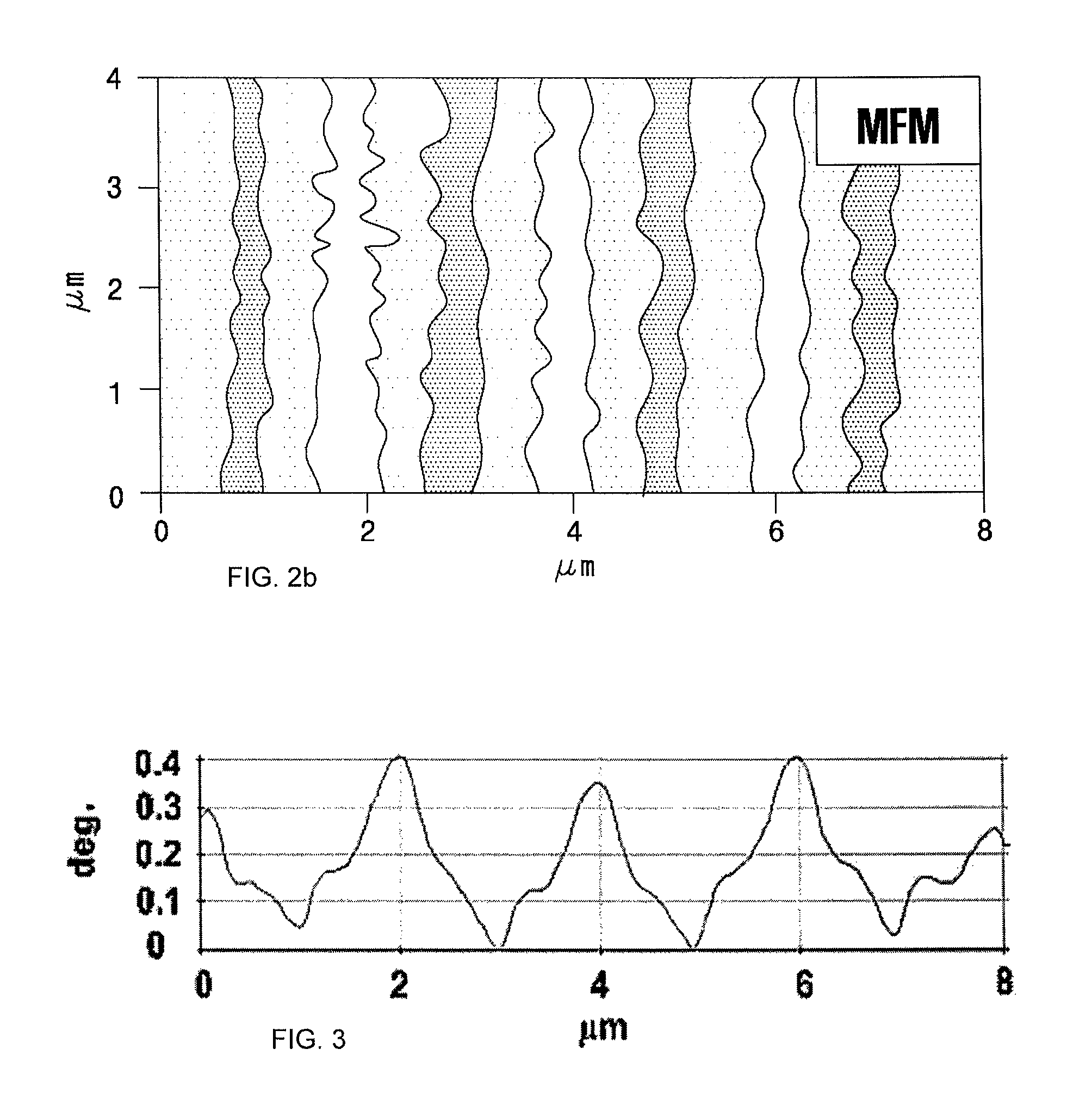
FIGS. 2a and 2b show Atomic Force Microscopy (AFM) and Magnetic Force Microscopy (MFM) images for one-dimensional spin photonic crystals prepared in Example 1.

Referring to FIGS. 2a and 2b, it can be seen that photonic crystals of Example 1-2 fabricated by using the selective-area annealing with the two-beam interference technique of femtosecond laser pulses have one-dimensional spin grating formed thereon. Particularly, the AFM image of FIG. 2a shows that the bright-band region with a relatively rough surface and the dark-band region with a relatively smooth surface were formed with the uniform fringe spacing on surfaces of the photonic crystals. Further, the corresponding MFM image in FIG. 2b shows that two regions having different properties (magnetic and nonmagnetic regions) were repeatedly and periodically formed on surfaces of the photonic crystals of Example 1. Further, the above microscopic images all exhibit clear formation of the boundary between the magneti...


PUM

PropertyMeasurementUnit
intersection angleaaaaaaaaaa
sizeaaaaaaaaaa
wavelengthaaaaaaaaaa

Abstract

Provided is a method for preparing a one-dimensional spin photonic crystal device and a one-dimensional spin photonic crystal device prepared by the same. The method comprises forming magnetic and nonmagnetic regions by the interference of laser beams generated from a femtosecond laser light source. The method of the present invention enables production of one-dimensional spin photonic crystals having excellent properties by a rapid and simple process, and is therefore suitable for high integration and large-scale production of desired devices. Further, the prepared photonic crystals exhibit excellent magneto-optical effects and are therefore applicable to development of novel optical devices, and the like.

Description

BACKGROUND OF THE INVENTION1. Field of the InventionThe present invention relates to a method for preparing a one-dimensional spin photonic crystal device and a one-dimensional spin photonic crystal device prepared by the same. More specifically, the present invention relates to a method for preparing a one-dimensional spin photonic crystal device, which enables fabrication of a one-dimensional spin photonic crystal device having excellent properties by an inexpensive and efficient method, and a one-dimensional spin photonic crystal device prepared by the same.2. Description of the Related ArtA great deal of attention has recently been focused on photonic crystals as a promising material necessary for the development of the next-generation optical communication devices such as nanolasers, superprisms capable of processing multiwavelength optical information, waveguides, and the like, and photon computers having ultra-high-speed information processing capacity (e.g. several tens of T...

Claims


Application Information

Patent Timeline
Patent Type & Authority Patents(United States)
IPC IPC(8): C23C14/00C23C14/32G03F1/00G03F7/00G02F1/09
CPCB82Y20/00C03C17/001C03C17/09C23C14/185C23C14/3414G02B6/1225C03C2217/27
Inventor LEE, YOUNG-PAKRHEE, JOO-YULLKIM, JIN-BAELEE, GEON-JOON
Owner IUCF HYU (IND UNIV COOP FOUND HANYANG UNIV)
Why Eureka
Try Eureka