Formulations for cleaning ion-implanted photoresist layers from microelectronic devices

a technology of photoresist layer and microelectronic device, which is applied in the direction of cleaning using liquids, inorganic non-surface active detergent compositions, instruments, etc., can solve the problems of physical and chemical rigidity, time-consuming and costly processes, and the rigid ion-implanted photoresist layer, also referred to as the carbonized region or “crust,” has been difficult to remove. , to achieve the effect of reducing the number of steps,

Inactive Publication Date: 2012-02-14
ADVANCED TECH MATERIALS INC
View PDF32 Cites 24 Cited by
  • Summary
  • Abstract
  • Description
  • Claims
  • Application Information

AI Technical Summary

Benefits of technology

[0018]Other aspects, features and embodiments of the invention will be more fully apparent from the ensuing disclosure and appended claims.

Problems solved by technology

Unfortunately, when high doses of ions (e.g., doses greater than about 1×10¹⁵ ions / cm2) are implanted in the desired layer, they are also implanted throughout the photoresist layer, particularly the exposed surface of the photoresist, which becomes physically and chemically rigid.
The rigid ion-implanted photoresist layer, also referred to as the carbonized region or “crust,” has proven difficult to remove.
As such, additional, complicated, time consuming and costly processes have been required to remove the ion-implanted photoresist layer because of the resulting low hydrogen concentration of the carbonized region.
Disadvantageously, however, wet strip treatments also etch the underlying silicon-containing layers, such as the substrate and gate oxide, and / or increase the gate oxide thickness.
As the feature sizes continue to decrease, satisfying the above cleaning requirements becomes significantly more challenging using the aqueous-based etchant formulations of the prior art.
Water has a high surface tension which limits or prevents access to the smaller image nodes with high aspect ratios, and therefore, removing the residues in the crevices or grooves becomes more difficult.
In addition, aqueous-based etchant formulations often leave previously dissolved solutes behind in the trenches or vias upon evaporative drying, which inhibits conduction and reduces device yield.
Furthermore, underlying porous low-k dielectric materials do not have sufficient mechanical strength to withstand the capillary stress of high surface tension liquids such as water, resulting in pattern collapse of the structures.
However, SCFs are highly non-polar and as such, many species are not adequately solubilized therein.
However, compositions containing only SCCO2 and co-solvents have proven to be incapable of removing 100% of the ion-implanted resist from the wafer surface.
In other words, the loss of greater than one Angstrom of said underlying silicon-containing layer is a substantial (greater than 10%), and unacceptable, over-etch of the underlying surface.

Method used


Image

  • Formulations for cleaning ion-implanted photoresist layers from microelectronic devices
  • Formulations for cleaning ion-implanted photoresist layers from microelectronic devices
  • Formulations for cleaning ion-implanted photoresist layers from microelectronic devices

Examples


example 1

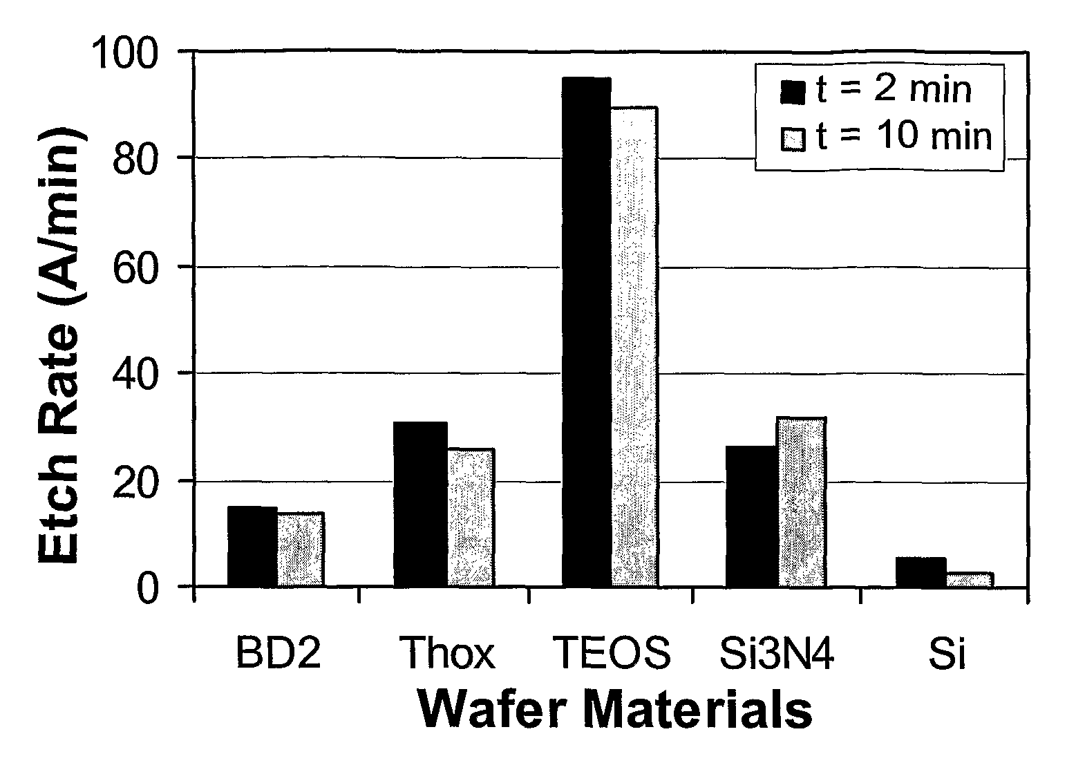
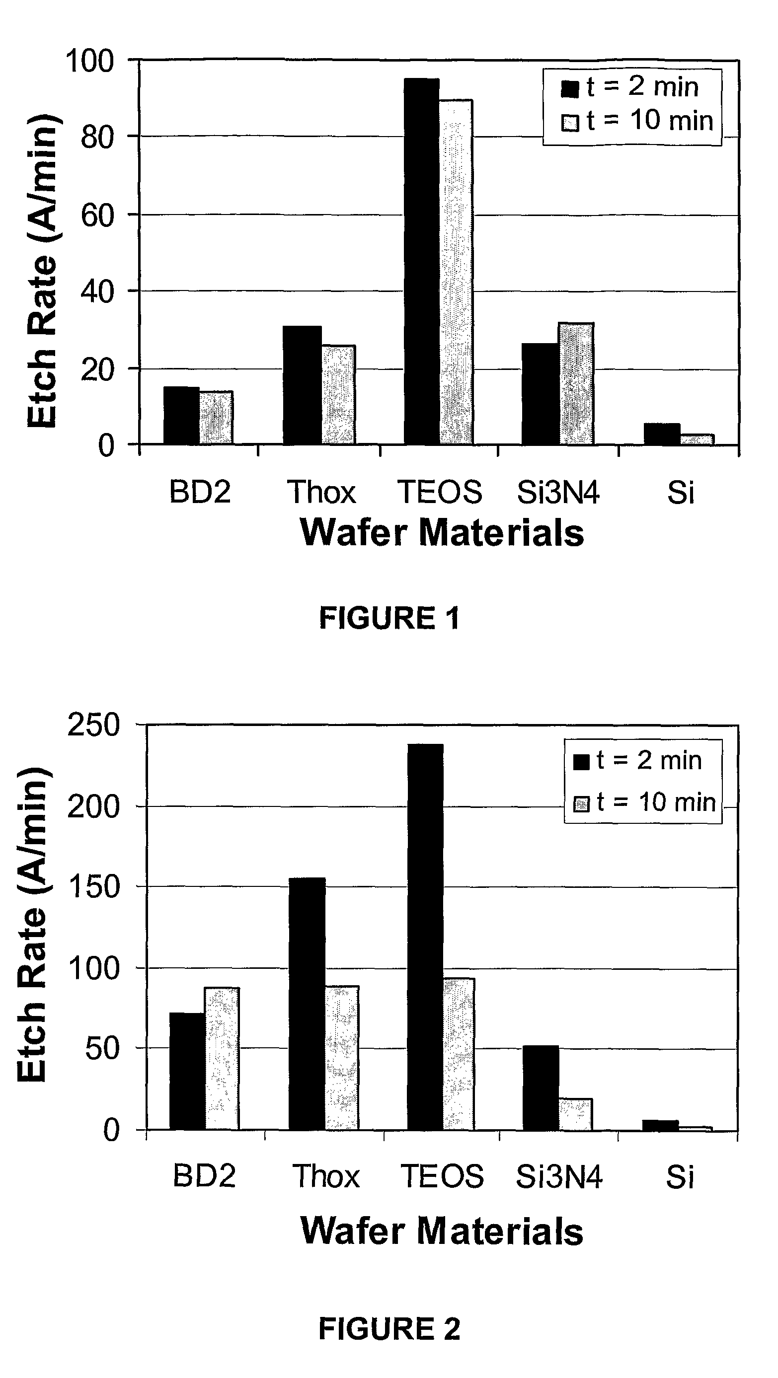
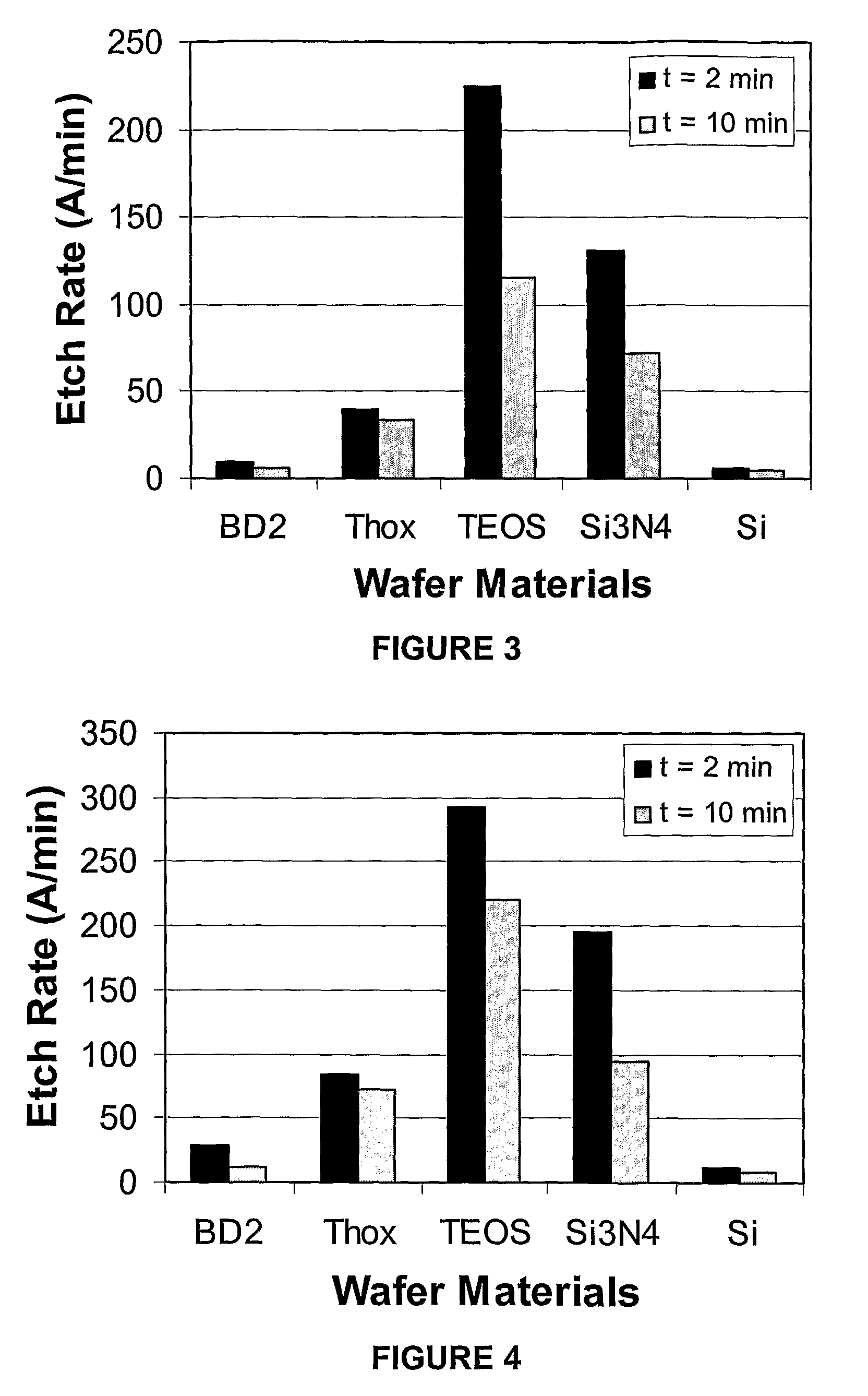
[0089]Dilute chelating agent (Lewis base / HF adducts) (0.4 g) was combined with 40 mL of a co-solvent to form compositions having a 1 w / v % of fluoride source for etch rate studies. The dilute Lewis base / HF adducts were prepared as follows. Commercially available Lewis base / HF adducts, specifically pyridine / HF (1:9) and triethylamine / HF (1:3), were diluted to 1:3, 1:1 and 3:1 (mol:mol) using the same Lewis base. To make pyridine / HF (1:3), 52 wt. % of pyridine / HF (1:9) and 48 wt. % anhydrous pyridine were combined. To make pyridine / HF (1:1), 27 wt. % of pyridine / HF (1:9) and 73 wt. % anhydrous pyridine were combined. To make pyridine / HF (3:1), 11 wt. % of pyridine / HF (1:9) and 89 wt. % anhydrous pyridine were combined. To make triethylamine / HF (1:1), 71 wt. % of triethylamine / HF (1:3) and 29 wt. % anhydrous triethylamine were combined. To make triethylamine / HF (3:1), 44 wt. % of triethylamine / HF (1:3) and 56 wt. % anhydrous triethylamine were combined. With dilute triethylamine / HF (1:...

example 2

[0095]The sample wafer examined in this study was a patterned silicon wafer including bulk and ion-implanted photoresist layers (see FIG. 5A). Various chemical additives, as described herein, were added to the dense fluid removal composition and removal efficiency of said composition evaluated. The dense fluid removal composition included 98.95 wt. % SCCO2, 1 wt % methanol, and 0.05 wt. % pyridine / HF complex (1:1 mole ratio). The temperature of the SCF-based composition was maintained at 70° C. throughout the removal experiments. The removal conditions included a static soak at 3,800 psi for 10 minutes described hereinabove. Following removal, the wafer was thoroughly rinsed first with copious amounts of SCCO2 / methanol and then with copious amounts of pure SCCO2, as described herein, in order to remove any residual solvent and / or precipitated chemical additives. FIG. 5B shows the result of this experiment, as described herein below.

[0096]FIG. 5A is a scanning electron micrograph (60...


PUM

PropertyMeasurementUnit
temperatureaaaaaaaaaa
pressureaaaaaaaaaa
thicknessaaaaaaaaaa

Abstract

A method and composition for removing bulk and ion-implanted photoresist and / or post-etch residue material from densely patterned microelectronic devices is described. The composition includes a co-solvent, a chelating agent, optionally an ion pairing reagent, and optionally a surfactant. The composition may further include dense fluid. The compositions effectively remove the photoresist and / or post-etch residue material from the microelectronic device without substantially over-etching the underlying silicon-containing layer(s) and metallic interconnect materials.

Description

CROSS-REFERENCE TO RELATED APPLICATIONS[0001]This application is filed under the provisions of 35U.S.C. §371 and claims the priority of International Patent Application No. PCT / US2006 / 014407 filed on 14 Apr. 2006, which claims priority to U.S. Provisional Patent Application No. 60 / 672,157 filed on 15 Apr. 2005, which are both hereby incorporated herein in their entireties.FIELD OF THE INVENTION[0002]The present invention relates to compositions useful for the removal of bulk and ion-implanted photoresist and / or post-etch residue from the surface of microelectronic devices, and methods of using said compositions for removal of same.DESCRIPTION OF THE RELATED ART[0003]As semiconductor devices has become more integrated and miniaturized, ion implantation has been extensively employed during front-end-of-line (FEOL) processing to accurately control impurity distributions in the microelectronic device and to add dopant atoms, e.g., As, B, P, In and Sb, to the exposed device layers. The c...

Claims


Application Information

Patent Timeline
Patent Type & Authority Patents(United States)
IPC IPC(8): B08B3/04C11D1/00C11D3/28C11D3/26
CPCC11D3/042C11D3/2086C11D3/245C11D3/28C11D3/30C11D3/3427C11D3/368C11D3/43C11D7/08C11D7/261C11D7/30C11D7/32C11D7/34C11D7/36C11D11/0047C11D7/3209C11D7/3218C11D7/3281H01L21/0279H01L21/265H01L21/3046H01L21/30604
Inventor VISINTIN, PAMELA M.KORZENSKI, MICHAEL B.BAUM, THOMAS H.
Owner ADVANCED TECH MATERIALS INC
Why Eureka
Try Eureka