Method for fabricating novel high-performance field-effect transistor biosensor based on conductive polymer nanomaterials functionalized with anti-VEGF adapter

a technology of conductive polymer nanomaterials and biosensors, which is applied in the direction of discharge tubes/lamp details, instruments, thermionic cathodes, etc., can solve problems such as sensitivity degradation, and achieve the effect of reducing the formation of holes and reducing the flow of electric curren

Active Publication Date: 2012-03-20
SEOUL NAT UNIV R&DB FOUND
View PDF5 Cites 14 Cited by
  • Summary
  • Abstract
  • Description
  • Claims
  • Application Information

AI Technical Summary

Benefits of technology

[0012]As a result of a variety of extensive and intensive studies and experiments to solve the problems as described above, the inventors of the present invention have developed a method, which is entirely different from known methods, that is, a method for fixing micro polymer nanomaterials through chemical bonding on an electrode substrate which is surface-modified with functional groups incorporated by copolymerization (Korean Patent Application No. 10-2007-0120359) and then developed biosensors for detecting VEGF with improved performance, as compared to conventional biosensors for diagnosing VEGF, based on the same. In addition, the present inventors confirmed that field-effect transistor array that remains stable in solution can be realized by adhering anti-VEGF aptamers to the surfaces of micro conductive polymer nanomaterials, to which functional groups are bound, through covalent bonding. The micro conductive polymer nanomaterials conventionally developed by the present inventors (Korean Patent Application No. 10-2007-0120359) have a diameter of about 200 nm, and field-effect transistor biosensors for diagnosing cancers provided with anti-VEGF aptamers developed by the present inventors exhibited about 10-fold improved sensitivity performance, as compared to conventional biosensors for detecting VEGF based on inorganic semiconductors (zinc nanowires). However, it was found that reuse of biosensors three or more times disadvantageously causes deterioration in sensitivity. The present inventors found that nanomaterials (100 nm) that are half the size (diameter) of conventional micro conductive polymers can be prepared by controlling the temperature and reaction time, and field-effect transistor biosensors for diagnosing cancers prepared using the same are selective to VEGF, exhibit 100-fold improved sensitivity, as compared to biosensors for detecting VEGF using conventional inorganic semiconductors, and maintained sensitivity, although reused ten or more times. The present invention has completed based on the discovery.
[0021]In step (a), the surfactant is dissolved in the nonpolar solvent at a temperature of −20° C. to 0° C. to form spherical micelles. The decrease in the diameter of micelles formed by reducing the activity of the surfactant at a low temperature enables diameter control of micro nanomaterials.
[0029]A carboxylic group (—COOH), the functional group in an amount controlled without undergoing complicated surface-modification processes can be readily incorporated into the surface of the micro conductive polymer nanomaterials prepared by the method according to the present invention. Micro conductive polymer nanomaterials are fixed by cross-linking bonds via amide bonds on the electrode substrate which is surface-modified into amine (—NH2) through silane treatment using the surface functional groups. The sensor device connected by these chemical bonds induces an increased interaction between the device and target materials due to inherent large surface-area and isotropic electrical properties of micro conductive polymer nanoparticles, and considerably rapid and reproducible reactions can be observed using the sensor device.
[0031]The field-effect transistor used in step (f) is already a well-known device, which is used for detecting electrical properties between the transducer and the target material in the present study. This detects variations in current characteristics between a source and a drain depending on variations in liquid-ion gate potential, when a predetermined voltage is applied between the source and the drain. Based on this mechanism, the device conductive polymer nanomaterials functionalized with an anti-VEGF aptamer are arranged as transducers between the source and the drain, and variations in source-drain electrical properties are detected through interaction between the transducer and a target material, when the target material is incorporated and serves as a gate potential. More specifically, the target material used in this research induces electric charges through interaction with the anti-VEGF aptamer, and these charges reduce formation of holes on the surfaces of conductive polymer nanomaterials, thus reducing flow of electric current between the source and drain.

Problems solved by technology

However, it was found that reuse of biosensors three or more times disadvantageously causes deterioration in sensitivity.

Method used


Image

  • Method for fabricating novel high-performance field-effect transistor biosensor based on conductive polymer nanomaterials functionalized with anti-VEGF adapter
  • Method for fabricating novel high-performance field-effect transistor biosensor based on conductive polymer nanomaterials functionalized with anti-VEGF adapter
  • Method for fabricating novel high-performance field-effect transistor biosensor based on conductive polymer nanomaterials functionalized with anti-VEGF adapter

Examples


example 1

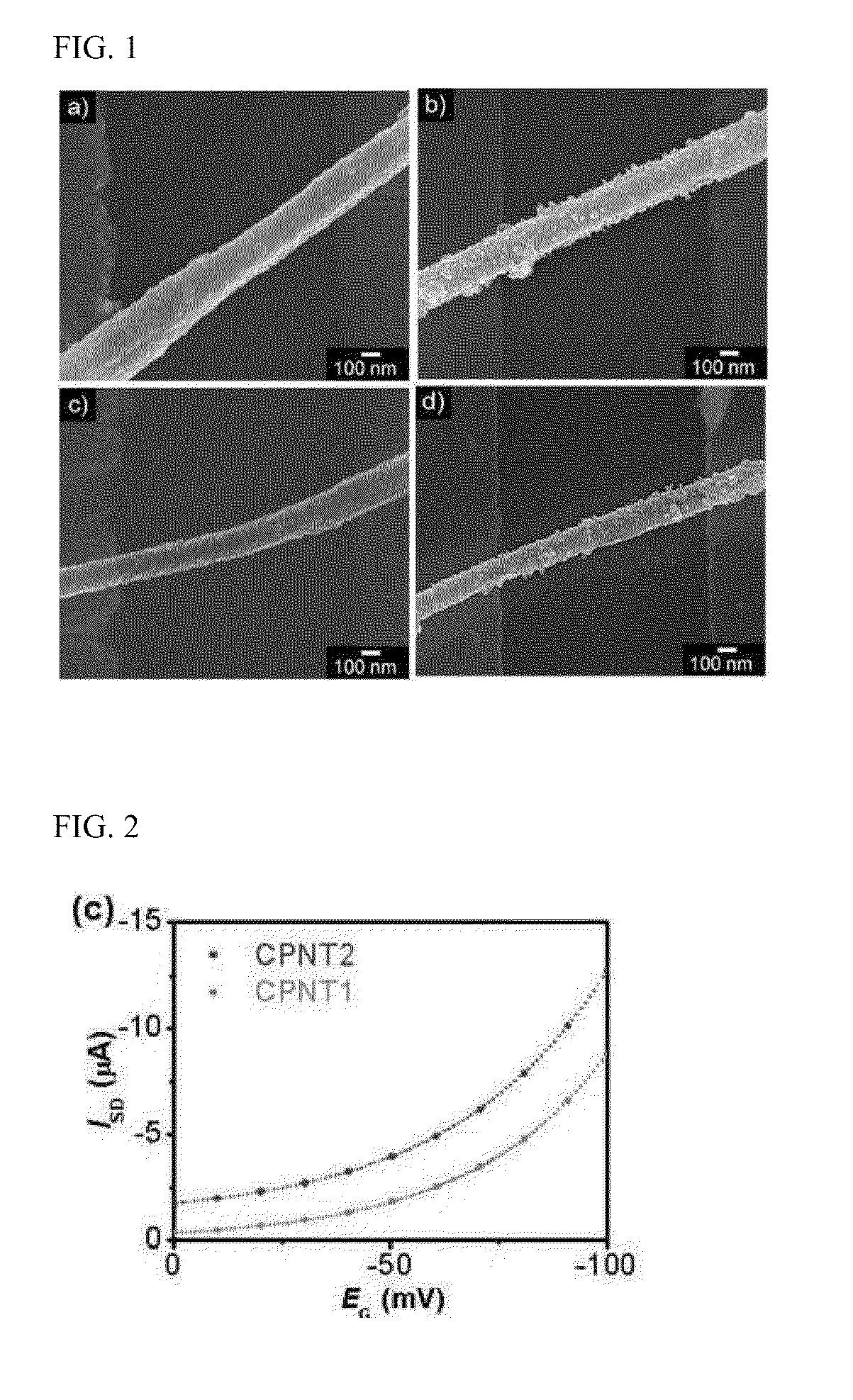
[0061]A reactor containing 20 mL of hexane was placed in a reactor vessel adjusted to −7° C. with a thermistor, 7.9 mmol of AOT was added thereto and the resulting mixture was stirred to form micelles. An aqueous ferric trichloride solution (7M, 0.5 mL) was incorporated into the reaction mixture and a mixture of pyrrole (6 mmol) and pyrrole-3-carboxylic acid (0.4 mmol) was then slowly added dropwise thereto. The resulting mixture was stirred at −4° C. for 48 hours to perform polymerization and an excess of ethanol was added to the reactor. The reaction solution was transferred to a separatory funnel and the precipitated carboxylated polypyrrole nanoparticle layer was then collected. The carboxylated polypyrrole nanoparticles thus prepared were observed with an electron microscope. As a result, nanotube particles having a diameter of about 100 nm and a length of 5 μm or higher were observed (FIG. (c)).

[0062]An interdigitated microelectrode array was patterned on a glass substrate by ...

experimental example 1

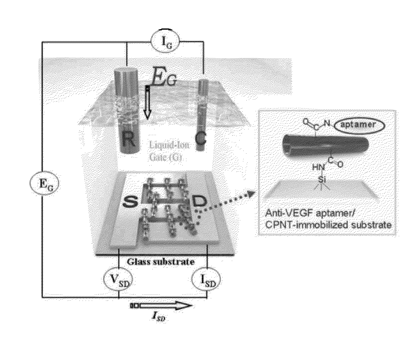
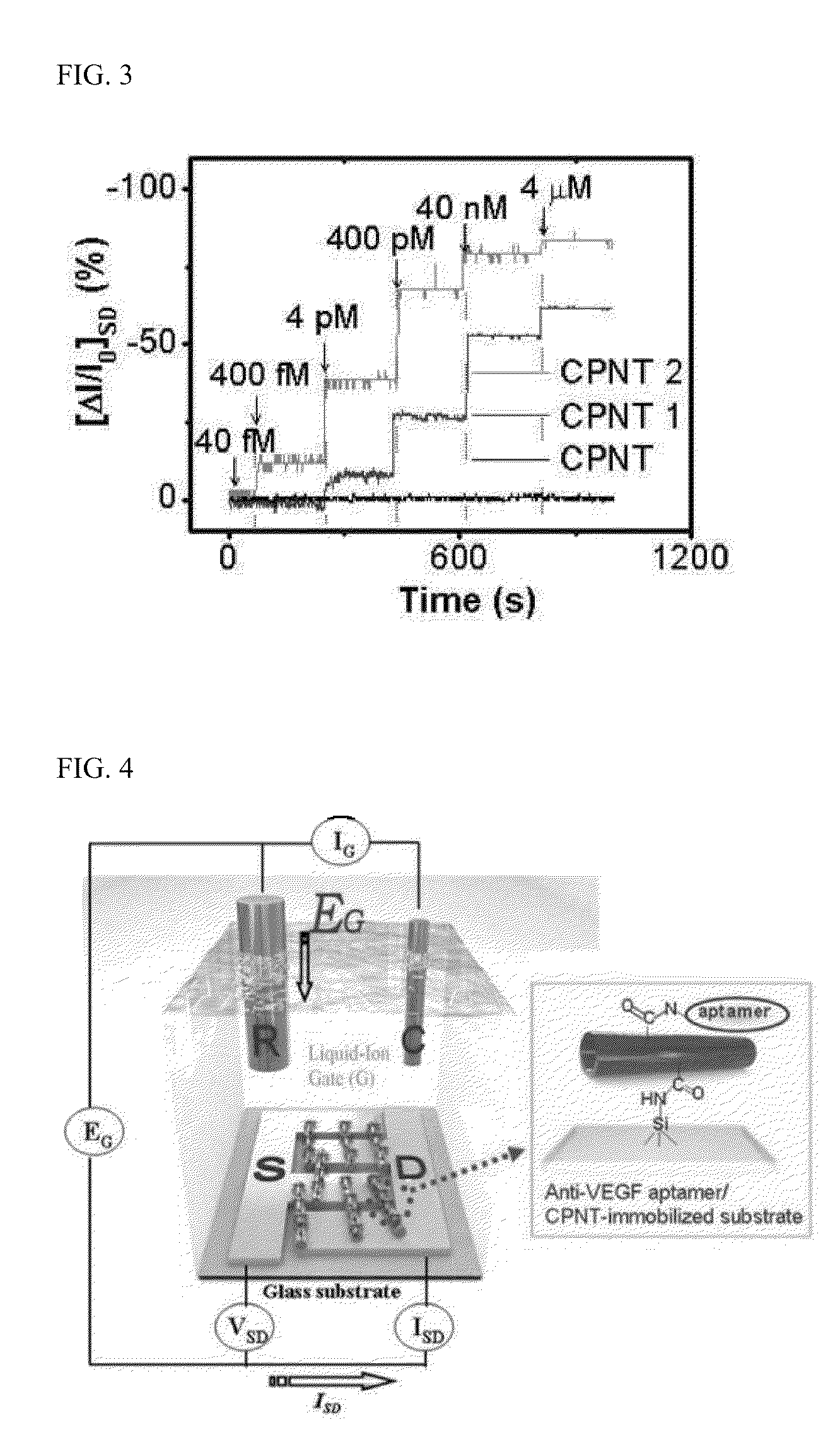
[0069]Regarding biosensors fabricated in Example 1 and Comparative Example 1, a channel region provided between a source (S) electrode and a drain (D) electrode was formed using carboxylated polypyrrole nanotubes. A source-drain voltage was applied using a potentiostat connected to a computer, and current variation (ΔI / I0=(I−I0) / I0, I and I0 indicate a current and an initial current value measured in real-time, respectively) was monitored in real time.

[0070]As a result, it was confirmed that the micro carboxylated polypyrrole nanotube (CPNT2) channel region fabricated at a lower temperature (Example 1), as compared to conventional cases exhibited higher conductivity than that of the nanomaterial (CPNT1) prepared in Comparative Example 1 (FIG. 2).

experimental example 2

[0071]To investigate the action of anti-VEGF aptamer for diagnosing cancers on biosensors fabricated in Example 1 and Comparative Example 1, polypyrrole nanotubes, to which anti-VEGF aptamer for diagnosing cancers was not adhered, were applied to the channel region. As a result, as shown in FIG. 3, when VEGF (Vascular Endothelial Growth Factor) was injected, no variation in source-drain current was observed. This means that selective reaction between anti-VEGF aptamer for diagnosing cancers and VEGF causes variation in source-drain current.


PUM

PropertyMeasurementUnit
sizeaaaaaaaaaa
diameteraaaaaaaaaa
temperatureaaaaaaaaaa

Abstract

Disclosed is a method for fabricating a high-performance field-effect transistor biosensor for diagnosing cancers using micro conductive polymer nanomaterials funtionalized with anti-VEGF aptamer. Disclosed is a high-sensitivity field-effect transistor biosensor for diagnosing cancers using a micro conductive polymer nanomaterial transistor array including a micro polymer nanomaterial transistor array including a channel region provided with a metal source electrode, a metal drain electrode, a gate and micro polymer nanomaterials, and an anti-VEGF aptamer covalently bound to the surface of the micro polymer nanomaterials constituting the channel region of the micro polymer nanomaterials transistor array, to target VEGF (Vascular endothelial growth factor).

Description

FIELD OF THE INVENTION[0001]The present invention relates to a method for preparing micro polymer nanomaterials, to which anti-VEGF aptamer selectively bound to vascular endothelial growth factors (VEGFs) is adhered, and a method for fabricating a high-performance field-effect transistor biosensor for diagnosing cancers using the conductive polymer nanomaterials. More specifically, the present invention relates to a method for detecting trace amounts of VEGF present in blood by fixing micropolymer nanomaterials, to which an anti-VEGF aptamer having high affinity to VEGF is chemically bound, on an electrode substrate and real-time monitoring current variation caused by the bond with VEGF in a field-effect transistor array.BACKGROUND OF THE INVENTION[0002]To date, biosensors have generally used optical measurement methods utilizing optical dyes. Biosensors using optical measurement methods have advantages of considerably excellent sensitivity and superior sensing selectivity, but disa...

Claims


Application Information

Patent Timeline
Patent Type & Authority Patents(United States)
IPC IPC(8): H01L21/00
CPCG01N33/5438G01N27/4145G01N27/4146Y10S977/742Y10S977/729Y10S977/716
Inventor JANG, JYONG SIKKWON, OH SEOKPARK, SEON JOO
Owner SEOUL NAT UNIV R&DB FOUND
Why Eureka
Try Eureka