Semiconductor device and production method therefor

a technology of semiconductor devices and production methods, applied in the direction of semiconductor devices, basic electric elements, electrical equipment, etc., to achieve the effects of enhancing area efficiency, reducing element isolation width, and reducing an area of an elemen

Active Publication Date: 2012-05-29
UNISANTIS ELECTRONICS SINGAPORE PTE LTD
View PDF26 Cites 59 Cited by
  • Summary
  • Abstract
  • Description
  • Claims
  • Application Information

AI Technical Summary

Benefits of technology

[0044]In view of the above problems, it is an object of the present invention to propose an SGT capable of higher integration and higher performance as compared with the conventional SGTs.
[0052]The semiconductor device of the present invention is capable of employing a substrate with an on-substrate dielectric film to facilitate a reduction in element isolation width, and stably forming a silicide layer for mutually connecting transistors, while forming a gate electrode around a pillar-shaped semiconductor layer in a self-alignment manner and with a desired film thickness. This simultaneously makes it possible to achieve element isolation capable of reducing an area of an element and enhancing area efficiency, a reduction in circuit occupancy area, a reduction in parasitic resistance and parasitic capacitance which would otherwise be increased along with a reduction in size, and enhanced flexibility in circuit design. Specifically, in a structure intended to mutually connect transistors in a diffusion layer formed in a planar semiconductor layer formed on a substrate with an on-substrate dielectric film, a stable silicide layer can be obtained by forming a silicide layer in an upper portion of the planar semiconductor layer. Based on this silicide layer, the resistance which would otherwise be increased along with a reduction in size can be reduced. Particularly, in a structure intended to mutually connect transistors having different conductivity types, the silicide layer capable of directly connecting diffusion layers having different conductivity types therethrough allows the transistors to be arranged closer to each other, so that an occupancy area of a circuit, such as an inverter circuit, can be significantly reduced as compared with conventional SGTs. In addition, the silicide layer capable of reducing the resistance which would otherwise be increased along with a reduction in size can minimize a need for arranging the transistors in positions closest to each other, so as to enhance flexibility in circuit design. Furthermore, the use of the substrate with an on-substrate dielectric film allows a parasitic resistance of a drain or source diffusion layer to be reduced.
[0053]According to the production method of the present invention, a gate electrode can be formed around a pillar-shaped silicon layer in a self-alignment manner and by a desired film thickness. This makes it possible to densely arrange a plurality of pillar-shaped silicon layers having different gate electrodes so as to reduce a circuit occupancy area. In addition, a process having sufficient process margin for forming a gate line can be established to facilitate gate line formation which has been a challenge in SGT.

Problems solved by technology

However, element isolation is achieved based on a LOCOS (local oxidation of silicon) technique, and consequently an element isolation width is increased to cause deterioration in area efficiency in an integrated circuit and difficulty in fully taking advantage of the area reduction effect of the SGT.
Moreover, in this SGT structure, it is necessary to reduce a resistance of the drain diffusion layer (1310, 1312), and, in cases where the drain diffusion layer (1310, 1312) is lined with a contact to reduce the resistance, the contact has to be formed on almost the entire region of a surface of the drain diffusion layer, which significantly restricts flexibility in laying lines in a first layer.
However, in the circuit having such a complicated layout, it is difficult to allow the source diffusion layer to be lined with a contact, and consequently a parasitic resistance of the source diffusion layer is increased to cause degradation in circuit performance.
Therefore, a process margin for forming the gate line is narrow, which causes difficulty in ensuring stable production.
Thus, in this SGT forming method, a process margin for forming the gate line becomes extremely narrow.
Therefore, an element isolation width is increased to cause deterioration in area efficiency in an integrated circuit, and difficulty in fully taking advantage of the area reduction effect of the SGT.
Generally, a silicide layer is low in thermal resistance.
In particular, nickel silicide (NiSi) employed in nano-devices since the 65-nm generation has an upper temperature limit of about 500 to 600° C. Thus, when the silicide layer is affected by an impurity activation heat treatment to be performed at about 1000° C. during transistor formation, an excessive reaction undesirably occurs therein to cause an increase in resistance and leak current.
In view of this, it is practically difficulty to ensure stable production based on the structure of this conventional example.
Moreover, due to the silicide layer 1543 located underneath the pillar-shaped silicon layer, silicon cannot be formed by epitaxial growth during crystal growth of the pillar-shaped silicon layer, to cause significant deterioration in transistor characteristics.
However, in this conventional example, a transistor is formed after forming the silicide layer, in the same manner as that in the conventional example illustrated in FIG. 128(b), and, due to the problem with the thermal resistance of the silicide layer, it is difficult to ensure stable production.
Moreover, due to the silicide layer 1563 located underneath the PMOS-forming pillar-shaped silicon layer, silicon cannot be formed by epitaxial growth during crystal growth of the PMOS-forming pillar-shaped silicon layer, to cause significant deterioration in transistor characteristics.
Nevertheless, this conventional example also involves a problem of a relatively large parasitic resistance in the source diffusion layer, causing degradation in circuit performance.
In this SGT forming method, if the contact hole for forming the pillar-shaped silicon layer, and a gate line pattern, are formed by a single lithography process, gate patterning becomes complicated, and it is significant difficult to form a gate electrode of an SGT to have a sufficiently small film thickness.
Generally, a sidewall of the contact hole has irregularities occurring during etching, and it is difficult to eliminate such irregularities.
Consequently, the irregularities are transferred to a surface of a channel region formed in the sidewall of the contact hole to cause deterioration in carrier mobility and difficulty in forming a high-performance transistor.
Moreover, considering that a size of the contact hole in currently produced LSIs in the 65-nm generation is about 80 nm, and the contact hole will become finer and finer in the future, it is difficult to form an epitaxial silicon film from the side of a bottom of such a fine contact hole, in adequate yield.Patent Document 1: JP 2-188966APatent Document 2: JP 7-99311ANon-Patent Document 1: S. Maeda, et al., “Impact of a Vertical Φ-Shape Transistor Cell for 1 Gbit DRAM and Beyond”, IEEE TRANSACTIONS ON ELECTRON DEVICES, December 1995, VOL.
Firstly, there remains a need for achieving a reduction in area of each element, and element isolation excellent in area efficiency, to reduce a circuit occupancy area.
Secondly, there remains a need for reducing a parasitic capacitance and a parasitic resistance of a source / drain region to improve transistor performance.
Thirdly, there remains a need for achieving a gate-line forming process having a wide process margin.

Method used


Image

  • Semiconductor device and production method therefor
  • Semiconductor device and production method therefor
  • Semiconductor device and production method therefor

Examples


first embodiment

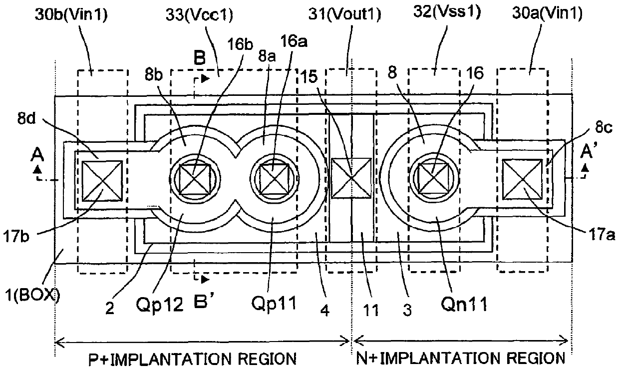
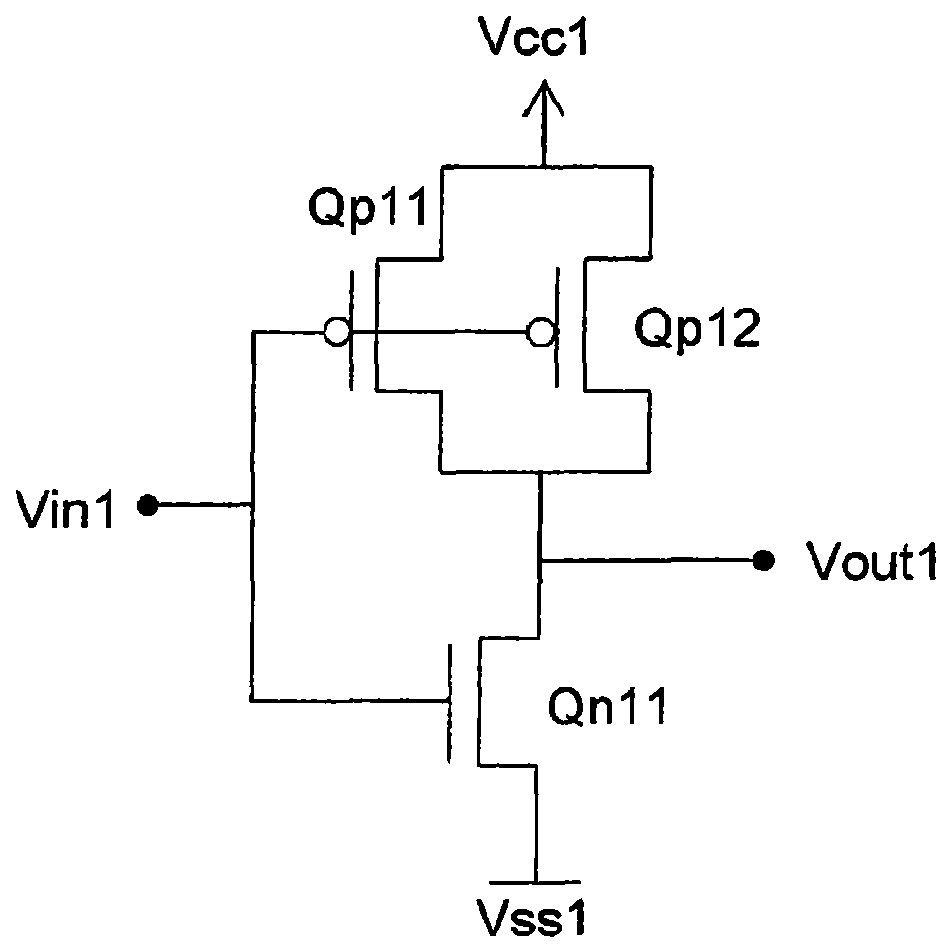
[0188]FIG. 1 is an equivalent circuit diagram of a CMOS inverter according to a first embodiment of the present invention. A circuit operation of the CMOS inverter will be described below. An input signal Vin 1 is applied to a gate of an NMOS Qn 11 and respective gates of two PMOSs Qp 11, Qp 12. When the Vin 1 is “1”, the NMOS Qn 11 is placed in an ON state, and each of the PMOSs Qp 11, Qp 12 is placed in an OFF state, so that an output signal Vout 1 becomes “0”. Reversely, when the Vin 1 is “0”, the NMOS Qn 11 is placed in an OFF state, and each of the PMOSs Qp 11, Qp 12 is placed in an ON state, so that the Vout 1 becomes “1”. As above, the CMOS inverter is operable to allow the output signal Vout 1 to have a value opposite to that of the input signal Vin 1.

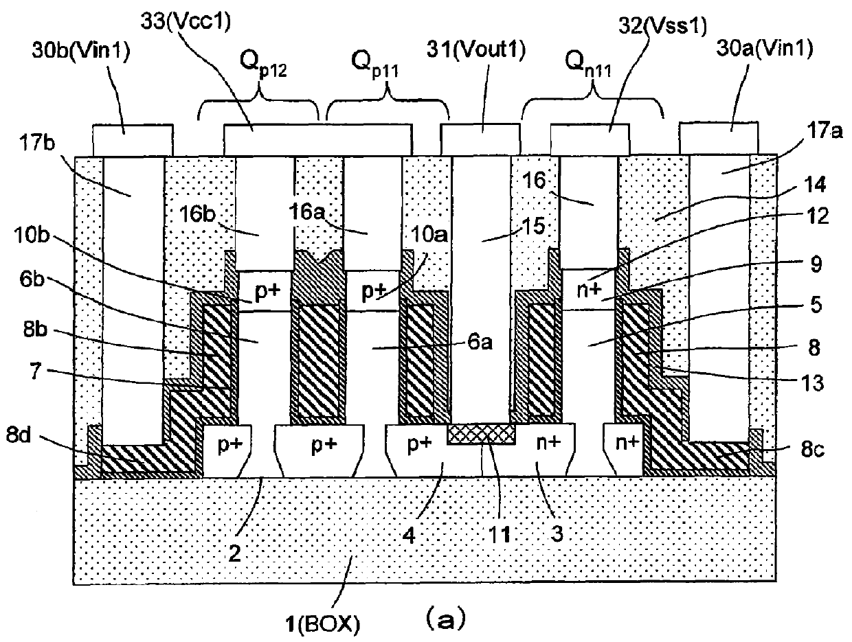
[0189]FIG. 2 is a top plan view of the CMOS inverter according to the first embodiment. FIGS. 3(a) and 3(b) are sectional views taken along the cutting-plane line A-A′ and the cutting-plane line B-B′ in FIG. 2, respectively. Wi...

second embodiment

[0236]A second embodiment of the present invention shows one example of a CMOS inverter made up using an SGT with a structure where a silicide layer is formed over the entire surface of drain diffusion layers formed in a planar silicon layer, and on a source diffusion layer formed in an upper portion of a pillar-shaped silicon layer. As a result of forming a silicide layer over the entire surface of the drain diffusion layers formed in the planar silicon layer, a parasitic resistance of the drain diffusion layers can be reduced. In addition, as a result of forming a silicide layer on the source diffusion layer formed in the upper portion of the pillar-shaped silicon layer, a parasitic resistance of the source diffusion layer can be reduced. The silicide layers to be formed on the drain diffusion layer and the source diffusion layer can be formed only on the drain diffusion layer and the source diffusion layer through a single process in a self-alignment manner.

[0237]FIG. 32 is an eq...

third embodiment

[0256]A third embodiment of the present invention shows one example of an SGT having a structure where a single contact is formed on tops of two or more pillar-shaped silicon layers in such a manner as to be shared by the pillar-shaped silicon layers.

[0257]FIG. 43 is an equivalent circuit diagram of a CMOS inverter according to the third embodiment. A circuit operation of the CMOS inverter is the same as that in the second embodiment, and its description will be omitted here.

[0258]FIG. 44 is a top plan view of the CMOS inverter according to the third embodiment. FIGS. 45(a) and 45(b) are sectional views taken along the cutting-plane line A-A′ and the cutting-plane line B-B′ in FIG. 44, respectively.

[0259]The third embodiment is different from the second embodiment in that, in the third embodiment, source diffusion layers formed in respective upper portions of adjacent two pillar-shaped silicon layers 306a, 306b forming PMOSs Qp 41, Qp 42, are connected to each other through a rectan...


PUM


Abstract

It is intended to provide a semiconductor device including a MOS transistor, comprising: a semiconductor pillar; one of a drain region and a source region formed in contact with a lower part of the semiconductor pillar; a first gate formed around a sidewall of the semiconductor pillar through a first dielectric film therebetween; and an epitaxial semiconductor layer formed on a top surface of the semiconductor pillar, wherein the other of the source region and the drain region is formed so as to be at least partially in the epitaxial semiconductor layer, and wherein: the other of the source region and the drain region has a top surface having an area greater than that of the top surface of the semiconductor pillar.

Description

RELATED APPLICATIONS[0001]Pursuant to 35 U.S.C. §119(e), this application claims the benefit of the filing date of Provisional U.S. Patent Application Ser. Nos. 61 / 207,567 filed on Feb. 13, 2009 and 61 / 217,896 filed on Jun. 4, 2009. This application is a continuation application of PCT / JP2009 / 051459 filed on Jan. 29, 2009 which claims priority under 35 U.S.C. §365(a) to PCT / JP2008 / 051300 filed on Jan. 29, 2008 and JP2009-109126 filed on Apr. 28, 2009. The entire contents of these applications are hereby incorporated by reference.TECHNICAL FIELD[0002]The present invention relates to a semiconductor device and a production method therefor, and more particularly to a structure and a production method for an SGT (Surrounding Gate Transistor) which is a vertical MOS transistor comprising a pillar-shaped semiconductor layer having a sidewall serving as a channel region, and a gate electrode formed to surround the channel region.BACKGROUND ART[0003]With a view to achieving higher integrati...

Claims


Application Information

Patent Timeline
Patent Type & Authority Patents(United States)
IPC IPC(8): H01L29/78
CPCH01L21/84H01L27/1203H01L29/78642
Inventor MASUOKA, FUJIOARAI, SHINTARO
Owner UNISANTIS ELECTRONICS SINGAPORE PTE LTD
Why Eureka
Try Eureka