
Light-emitting nanocomposite particles

a technology of nanocomposite particles and light-emitting layers, which is applied in the direction of electric lighting sources, semiconductor devices, and light sources. it can solve the problems of high manufacturing cost, high cost and rigid substrates, and difficulty in combining multi-color output from the same chip, so as to enhance enhance the electrical connection. effect, the effect of enhancing the conductivity of the light-emitting layer

Inactive Publication Date: 2013-01-29
NANOCO TECH LTD
View PDF13 Cites 10 Cited by
  • Summary
  • Abstract
  • Description
  • Claims
  • Application Information

AI Technical Summary

Benefits of technology

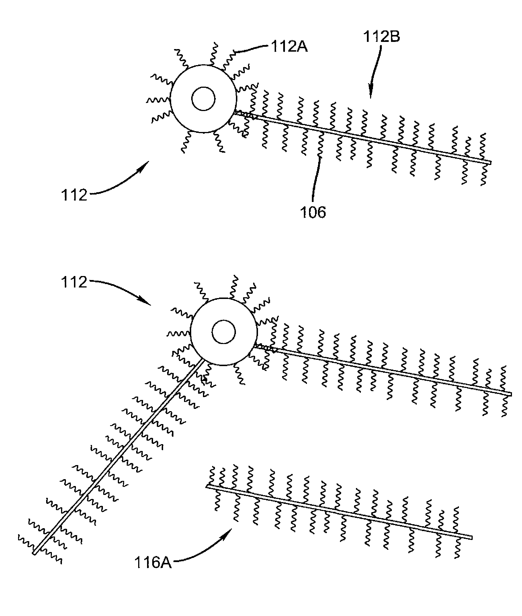
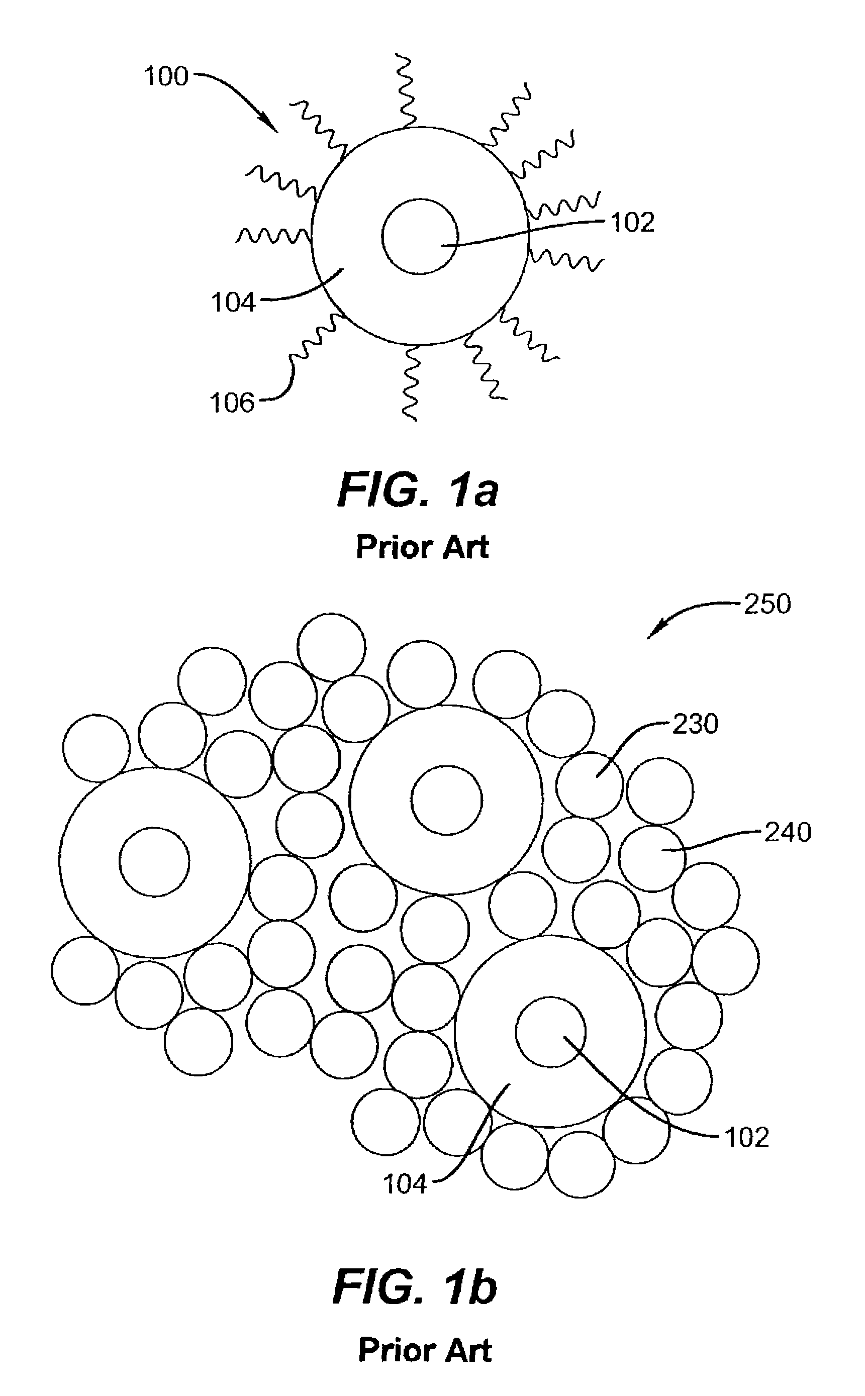
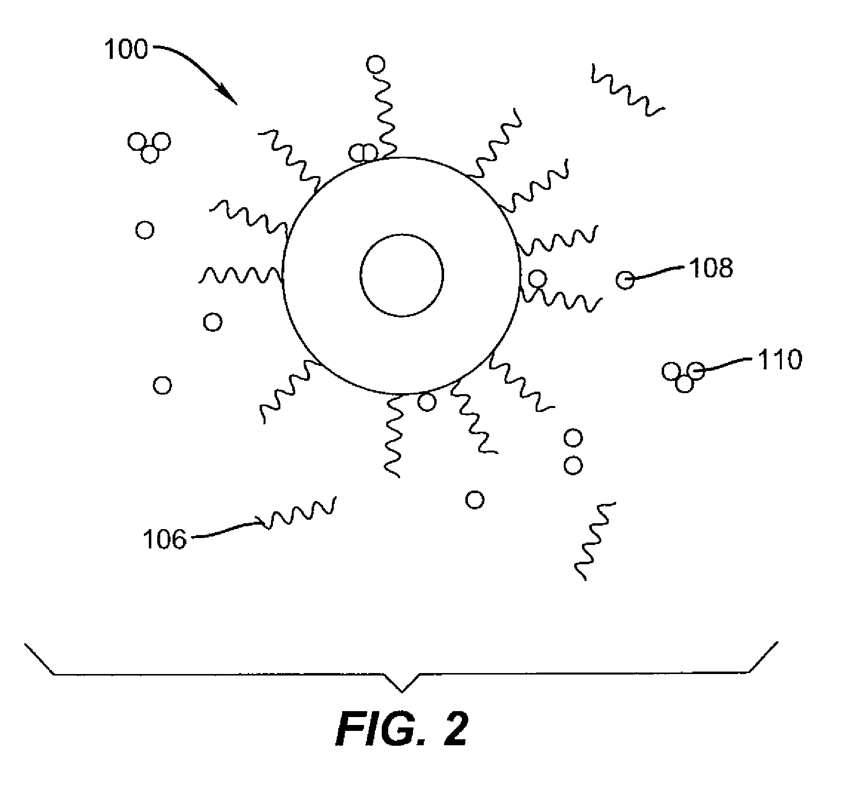
The present invention provides a way to create a light-emitting layer that is simultaneously luminescent and conductive using quantum dots. This layer includes a composite of conductive nanoparticles and shelled quantum dot emitters connected to the nanoparticles. By using a thermal anneal, the conductivity of the layer is enhanced and electron-hole injection into the quantum dots is enhanced. To protect the quantum dots from losing their fluorescent efficiency, the quantum dot shells are engineered to confine the electrons and holes, such that, their wave functions do not sample the surface states of the outer inorganic shell. The resulting all inorganic light-emitting diode device is low cost, can be formed on a range of substrates, and can be tuned to emit over a wide range of visible and infrared wavelengths. Its brightness should be enhanced and its encapsulation requirements should be reduced compared to organic-based light emitting diode devices.

Problems solved by technology

The dominant ones are high manufacturing costs, difficulty in combining multi-color output from the same chip, and the need for high cost and rigid substrates.
In comparison to crystalline-based inorganic LEDs, OLEDs have much reduced brightness (mainly due to small carrier mobilities), shorter lifetimes, and require expensive encapsulation for device operation.
Because of problems, such as, aggregation of the quantum dots in the emitter layer, the efficiency of these devices was rather low in comparison with typical OLED devices.
The efficiency was even poorer when a neat film of quantum dots was used as the emitter layer (Hikmet et al., J. Appl. Phys. 93, 3509 (2003)).
The poor efficiency was attributed to the insulating nature of the quantum dot layer.
Regardless of any future improvements in efficiency, these hybrid devices still suffer from all of the drawbacks associated with pure OLED devices.
The resulting device had a poor external quantum efficiency of 0.001 to 0.01%.
These organic ligands are insulators and would result in poor electron and hole injection onto the quantum dots.
In addition, the remainder of the structure is costly to manufacture due to the usage of electron and hole semiconducting layers grown by high vacuum techniques, and the usage of sapphire substrates.
Organic linking agents are poor conductors of electrons and holes.
Thus, Alivisatos et al. does not provide a sufficient means of conducting carriers into the light-emitting layer and further into the quantum dots in order to achieve efficient light emission.
The light-emitting layer is incorporated into an LED, however, the light-emission obtained is not sufficiently high since the method of Su et al. also does not provide a good means for conduction of electrons and hole within the light-emitting layer and into the quantum dot emitters.
Ligand exchange requires separation of quantum dots from a solvent, which can be difficult, since the quantum dots are extremely small.
For example, attempts to separate quantum dots by centrifugation of a colloid dispersion may precipitate only a fraction of the dots, even after prolonged times. In addition, if very high centrifugation speeds are employed, it can be very difficult to re-disperse the resulting tightly-packed quantum dot precipitate.

Method used


Image

  • Light-emitting nanocomposite particles
  • Light-emitting nanocomposite particles
  • Light-emitting nanocomposite particles

Examples


example 1

Preparation of Light-Emitting Nanocomposite Particles and Formation of a Light-Emitting Layer

Preparation of Quantum Dots

[0088]CdSe / ZnSeS core shell quantum dots were prepared by the following procedure. Standard Schlenk line procedures were followed for the synthesis. CdSe cores were formed following the green synthesis procedure of Talapin et al. (D. V. Talapin et al., J. Phys. Chem. B108, 18826 (2004)). More specifically, 532 nm emitting CdSe cores were obtained after vigorously stirring the reaction mixture at 260° C. for 7.5 minutes. After cooling the CdSe crude solution back to room temperature, 4 ml of TOPO and 3 ml of HDA were added to 1.5 ml of crude solution (unwashed) in a Schlenk tube. After degassing the mixture at 110° C. for 30 minutes, the solution was brought up to 190° C. under argon overpressure and constant stirring. With the shell composed of ZnSeS, precursors of Zn, Se, and S were prepared in a dry box. The Zn precursor was 1 M diethylzinc in hexane, the Se prec...

example 2

Comparative Separation of Quantum Dots from a Solvent

[0095]A crude solution containing only core / shell quantum dots (the same ones used in Example 1), having nonvolatile TOPO, HDA, and TOP ligands, was ligand exchanged (exchange to pyridine ligand) in substantially the same manner as described in the first section of Example 1. No substantial problems were encountered in the first washing (with toluene and methanol). As such, a plug could be formed following centrifuging and the resulting supernatant was clear. Next pyridine was added as before and the mixture was stirred at 80° C. for 24 hours. Problems arose when the exchanged solution was washed with hexane (as before) and centrifuged to obtain a plug. Despite centrifuging at much greater rates than in Example 1, only a very small plug could be obtained. In fact, exposing the supernatant to UV light revealed that the majority of quantum dots remained in solution (greater than 75%).

[0096]Example 2 illustrates the difficulty of iso...


PUM

PropertyMeasurementUnit
temperatureaaaaaaaaaa
boiling pointaaaaaaaaaa
bandgap energy levelsaaaaaaaaaa

Abstract

A method of making an inorganic light emitting layer includes combining a solvent for semiconductor nanoparticle growth, a solution of core / shell quantum dots, and semiconductor nanoparticle precursor(s); growing semiconductor nanoparticles to form a crude solution of core / shell quantum dots, semiconductor nanoparticles, and semiconductor nanoparticles that are connected to the core / shell quantum dots; forming a single colloidal dispersion of core / shell quantum dots, semiconductor nanoparticles, and semiconductor nanoparticles that are connected to the core / shell quantum dots; depositing the colloidal dispersion to form a film; and annealing the film to form the inorganic light emitting layer.

Description

STATEMENT REGARDING FEDERALLY-SPONSORED RESEARCH OR DEVELOPMENT[0001]This invention was made with Government support under Cooperative Agreement #DE-FC26-06NT42864 awarded by DOE. The Government has certain rights in this invention.CROSS-REFERENCE TO RELATED APPLICATIONS[0002]Reference is made to commonly assigned U.S. patent application Ser. No. 11 / 668,041 filed Jan. 29, 2007, entitled “Doped Nanoparticle Semiconductor Charge Transport Layer” by Keith B. Kahen; U.S. patent application Ser. No. 11 / 677,794 filed Feb. 23, 2007, entitled “Ex-Situ Doped Semiconductor Transport Layer” by Keith B. Kahen; and U.S. patent application Ser. No. 11 / 678,734 filed Feb. 26, 2007, entitled “Doped Nanoparticle-Based Semiconductor Junction” by Keith B. Kahen, the disclosures of which are incorporated herein.BACKGROUND OF THE INVENTION[0003]Semiconductor light emitting diode (LED) devices have been made since the early 1960s and currently are manufactured for usage in a wide range of consumer and com...

Claims


Application Information

Patent Timeline
Patent Type & Authority Patents(United States)
IPC IPC(8): H01L21/00
CPCH05B33/145
Inventor KAHEN, KEITH B.
Owner NANOCO TECH LTD
Learn More