Logic system with resistance to side-channel attack by exhibiting a closed clock-data eye diagram

a logic system and eye diagram technology, applied in logic circuits, computer security arrangements, instruments, etc., can solve problems such as increasing current consumption, increasing power consumption, and rendering security worthless, and achieve the effect of improving the resistance of the logic system

Inactive Publication Date: 2013-04-23
DEAS ALEXANDER ROGER +1
View PDF7 Cites 26 Cited by
  • Summary
  • Abstract
  • Description
  • Claims
  • Application Information

AI Technical Summary

Benefits of technology

[0026]It is an objective of the present invention to reduce the sensitivity of logic systems to comprise from monitoring externally observable features, i.e. side channel attacks.
[0029]It is a further objective of the present invention to provide a clocking scheme for a synchronous logic system with improved security.
[0034]The randomisation of the output clock edges improves the resistance of the logic system to attack methods such as power supply current monitoring, electromagnetic field monitoring or very near field monitoring, as a means to gain an insight to the operation or contents of the system. When the effective clock eye diagram is closed by random jitter, there is provably no data content in the side-channels (current in the power supply, or electromagnetic emissions from the system).

Problems solved by technology

Techniques known as simple power analysis, differential power analysis and higher order differential power analysis have been used to reveal the private encryption key, thereby rendering the security worthless.
Such techniques also results in an increase of current consumption.
This method suffers from the requirement to have an on-card capacitor which may present a problem in terms of the card form-factor.
The other problem with this approach is that it makes it possible to monitor the emissions from the capacitor using near field probes, which are nicely identified for the attacker simply by the switch in power.
This method suffers from increased power consumption as well as not being suitable for the highest level of integration by using components that are non-standard in VLSI standard CMOS processes.
There are other disadvantages and weaknesses created by this method.
However, all of these methods rely on one or more of the following; balancing edge speed of the inputs, generating equal delays for the true output and complementary output rising edges, and balancing the load capacitance which also includes balancing the routing capacitance.
Any imbalance reduces the effectiveness of the differential gate in generating constant amplitude current spikes thereby allowing an intruder to simply increase the complexity of the averaging algorithm to obtain the knowledge sought.
These differential systems can be compromised simply by reducing the supply voltage to the point where the differential pair saturates.
The method takes a lot of power as it is a linear power supply, and it has a high bandwidth.
Yet further, the use of linear power supplies implies increased current consumption.
A common issue with all of the above methods is that there may be one or more penalties associated with the implementation namely power consumption, circuit processing speed or area increase.
Randomising the position of current peaks reduces the ability of the intruder to align successive power consumption or current consumption traces.
However, to modulate the clock frequency it is necessary to operate the system at a lower overall frequency than is possible with modulation, and the reduction in frequency is not generally beneficial.
Further, in order to modulate the temporal position of current peaks over a wide time it is necessary to lower the clock frequency significantly which has ramifications on the overall performance of a system.
In general, it is desirable to be able to modulate the system clock with minimal impact to the speed of the logic system but solutions known in the prior art that use spread spectrum clocking do not achieve that.
There exists no possibility of applying random modulation to the system clock as a random function is two-sided and would result in the clock period being less than the minimum allowed.
In this example the clock period must be increased to 100 ns i.e. a reduction in operating frequency from 50 MHz to 10 MHz which is a significant penalty in operational speed and eye closure is not achieved.
Any systems with either internal clocks, or an external clock supplemented by an internal clock for the encryption engine can be compromised using a very near field probe.
The use of such a low amount of modulation has little impact on improving the security since such techniques do not close the clock eye diagram.
Accordingly, techniques such as spread spectrum clock generation do not provide much improvement in resistance against side-channel attacks.
Each foregoing prior art counter-attack methods has one or more of the following drawbacks in an integrated circuit or other physical implementation of an encryption engine: insufficient protection, large physical size, high power consumption, non-standard design flow, library availability to the implementation of a robust and practical encryption engine with high immunity to attack through simple, differential power analysis or higher order differential power analysis.

Method used


Image

  • Logic system with resistance to side-channel attack by exhibiting a closed clock-data eye diagram
  • Logic system with resistance to side-channel attack by exhibiting a closed clock-data eye diagram
  • Logic system with resistance to side-channel attack by exhibiting a closed clock-data eye diagram

Examples


Embodiment Construction

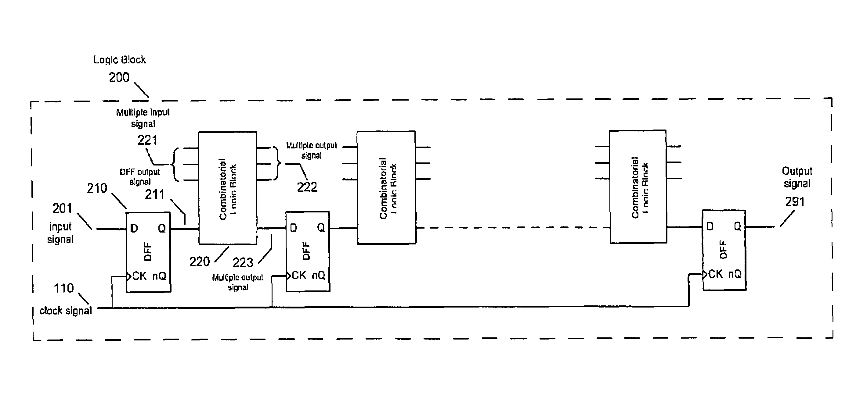
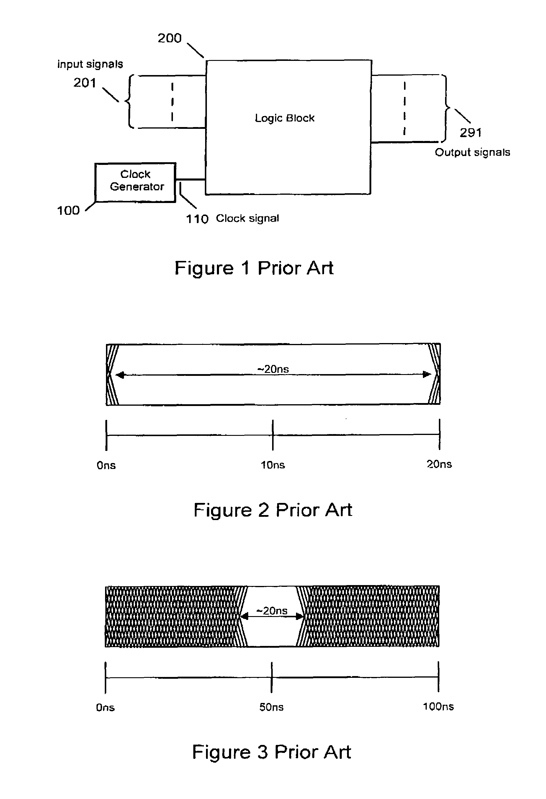
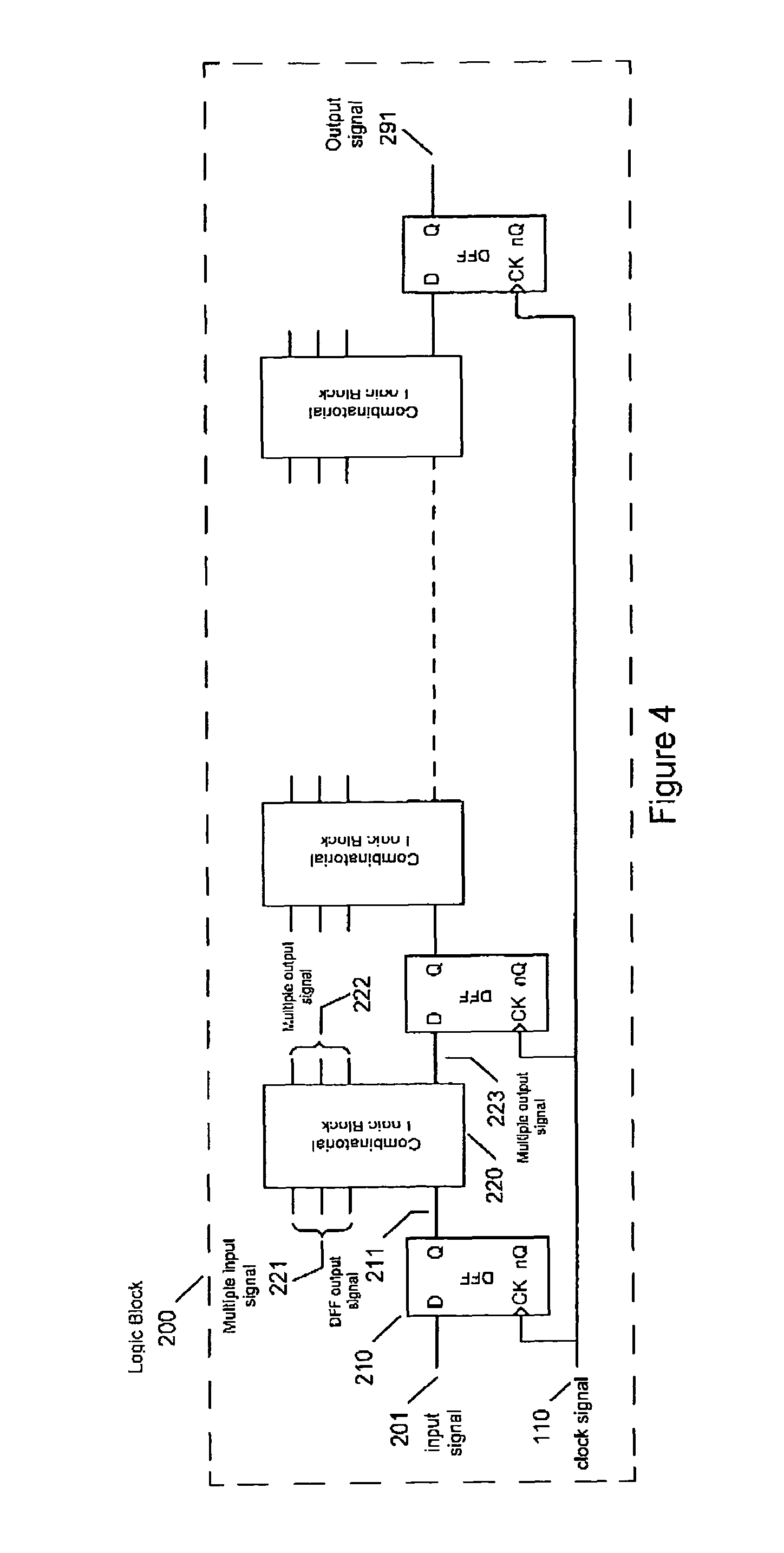
[0050]FIG. 1 shows a diagram of a synchronous logic system employed in the present invention. Clock generator 100 produces clock signal 110 for synchronous logic block 200 comprising one or more input signals 201 and generating one or more output signals 291. Output signals 291 may change state in response to input signals 201 at transitions of the input clock 110 based on the present and previous state of input signals 201, output signals 291, signals from internally stored states or a combination of one or all of these signals. For clarity of description, the present invention will refer to rising edge clock transitions but it will be clear to any person skilled in the art of logic design that the technique can be applied to logic systems can operate on falling edge clock transitions or both rising and falling clock edge transitions.

[0051]Where the synchronous logic systems depicted in FIG. 1 employ standard CMOS logic gates both systems will produce current peaks that may enable ...


PUM


Abstract

An improvement in the security of a logic system by minimizing observable features such as the power supply or electromagnetic radiation, so called, “side-channel attacks”. Specifically, the present invention comprises a technique and methods for reducing the ability of an intruder to monitor the relationship between currents in the system and the data in the system through the use of a randomized clock wherein the clock eye diagram is closed and without significant reduction in maximum operating speed compared to the reduction in maximum operating frequency that occurs when using conventional means of additive jitter. A system where the clock eye diagram is completely closed is provably more secure than systems where the clock eye diagram is partially open.

Description

BACKGROUND OF THE INVENTION[0001]1. Technical Field[0002]The present invention relates to providing security to a logic system from attack through monitoring of observable features such as the power supply or electromagnetic radiation, in so called “side-channel attacks”. A side-channel attack may seek to obtain information concerning the contents of the system, such as a private key or crypto-engine data.[0003]Any system that has a partially open clock data eye is susceptible to side-channel attack. It is not sufficient to close the eye partially: it must be fully closed to be secure. It is also not sufficient to add noise to a clock or data emitter to disguise the signal: statistical analysis of a noisy eye can determine very quickly what the data is with the noise removed. For a system to be secure from side channel attack, the emissions must be completely random, and this requires a closed clock eye diagram. Attempts described in the prior art other than a co-pending application...

Claims


Application Information

Patent Timeline
Patent Type & Authority Patents(United States)
IPC IPC(8): H03K19/00H03K3/00
CPCH04L9/003G06F21/725G06F21/558G06F21/755
Inventor DEAS, ALEXANDER ROGERCOYNE, DAVID
Owner DEAS ALEXANDER ROGER
Why Eureka
Try Eureka