Layer transfer of films utilizing thermal flux regime for energy controlled cleaving

a technology of thermal flux and film transfer, applied in the field of film transfer of thermal flux regime for energy controlled cleaving, can solve the problems of poor carrier life, many limitations of solar cells, and difficult manufacturing of materials for solar cells, and achieve the effects of high efficiency, reduced kerf loss, and high quality

Inactive Publication Date: 2014-01-28
SILICON GENERAL CORPORATION
View PDF4 Cites 7 Cited by
  • Summary
  • Abstract
  • Description
  • Claims
  • Application Information

AI Technical Summary

Benefits of technology

[0012]Many benefits can be obtained by implementing the present invention. In a preferred embodiment, single crystal silicon ingot substrate with a surface plane in a {100}, {111} or {110} crystallographic plane can be selected. Thus, the (H) ion implantation for creating cleave region can be substantially limited to a low dose implantation with relative higher dose (the initiation dose) only on a portion of peripheral region to form a cleave initiation region. This substantially simplifies the layer transfer process, reduces system energy cost and enhances high volume manufacturability.
[0013]In certain embodiments, the layer transfer process is divided into (i) an initiation process utilizing a cleave initiation region formed by higher implant dose in a relatively small area of the silicon ingot substrate to initiate a fracture or form a cleave front, and (ii) a propagation process that extends the cleave front through the remainder of the silicon ingot substrate to release the film. In one embodiment, the cleave initiation region can be created using patterned implantation by irradiating high energy ionic particles with controlled dosage generated using a linear accelerator. Since the propagation process must extend the initiation region through the majority of the surface area of the film to be released, this process should operate reliably with a small implant dose, and perhaps without any dose. This is called the propagation dose, and the total dose needed for the process would therefore be the weighted area average of the initiation and propagation dose. For example, if the initiation area is 1% of the total area and utilizes 6×1016 cm−2 hydrogen while the propagation area utilizes 1×1016 cm−2 hydrogen, the total effective dose is 0.01*6×1016 cm−2+0.99*1×1016 cm−2 or 1.05×1016 cm−2. Reducing or even eliminating the propagation dose will have a first order effect on the total dose requirement for this cleaving process.
[0018]Utilizing embodiments of the present invention, a high quality film of crystalline material having a thickness ranging from a few tens of microns to a few hundreds of microns, can be produced with kerf loss substantially lower than possible utilizing conventional techniques. The resulting single crystal silicon thick films are particularly suited for use in high efficiency (20% or higher) photovoltaic cells. Embodiments of the present invention further provide a method for utilizing a controlled thermal flux for cleave initiation and guiding cleave front propagation in a rapid and precise manner. The method utilizes a surface temperature mapping to provide one or more feedback signal for scanning the beam spot and adjusting beam intensity of thermal flux to achieve the controlled propagation. Furthermore, the method allows automatic detection of cleave failure, undesired cracking, or film breakage etc. Some embodiments can utilize existing manufacture processing systems and techniques, and take some advantage of certain newly developed techniques for manufacturing thin wafer / substrate for various semiconductor device applications. For example, embodiments of the present invention support H-plane cleaving with low propagation dose, is essentially non-contact, operates using low thermal-budget, is production throughput compatible, has low maintenance requirements and is scalable to most film thickness required by both semiconductor and solar industries. More details about various embodiments of the present invention can be found in the description below.

Problems solved by technology

Unfortunately, such petroleum sources have become depleted and have lead to other problems.
Although effective, these solar cells still have many limitations.
Amorphous silicon is not a form of silicon commonly used in wafered solar cells due to its poor carrier lifetime in thicknesses less than a few microns.
The materials for solar cells are often difficult to manufacture.
Although these plates may be formed in a cost effective manner using crystallization furnaces, they do not possess optimum properties for highly effective solar cells.
In particular, polysilicon plates do not exhibit the highest possible efficiency in capturing solar energy and converting the captured solar energy into usable electrical power.
Such single crystal silicon is, however, expensive to manufacture and is also difficult to use for solar applications in an efficient and cost effective manner.
Additionally, both polysilicon and single-crystal silicon materials suffer from material losses during conventional manufacturing single crystal silicon substrates, where a sawing process is used to physically separate thin single crystal silicon layers from a single crystal silicon ingot originally grown.
This is a highly inefficient method of preparing thin polysilicon or single-crystal silicon plates for solar cell use.
Thin film solar cells are often less expensive by using less silicon material or alternative materials but their amorphous or polycrystalline structure are less efficient than the more expensive bulk silicon cells made from single-crystal silicon substrates.

Method used


Image

  • Layer transfer of films utilizing thermal flux regime for energy controlled cleaving
  • Layer transfer of films utilizing thermal flux regime for energy controlled cleaving
  • Layer transfer of films utilizing thermal flux regime for energy controlled cleaving

Examples


Embodiment Construction

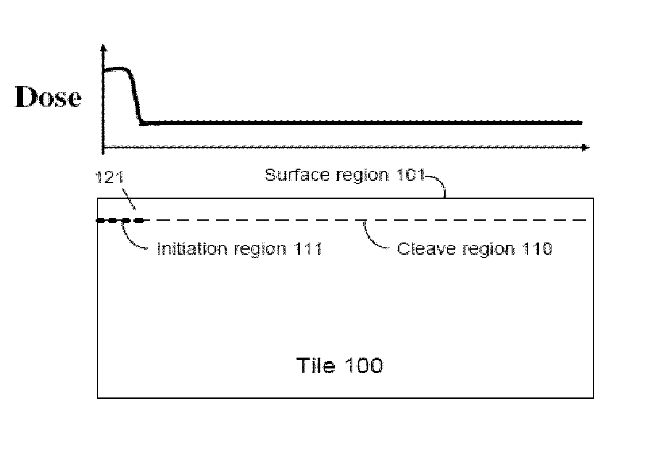
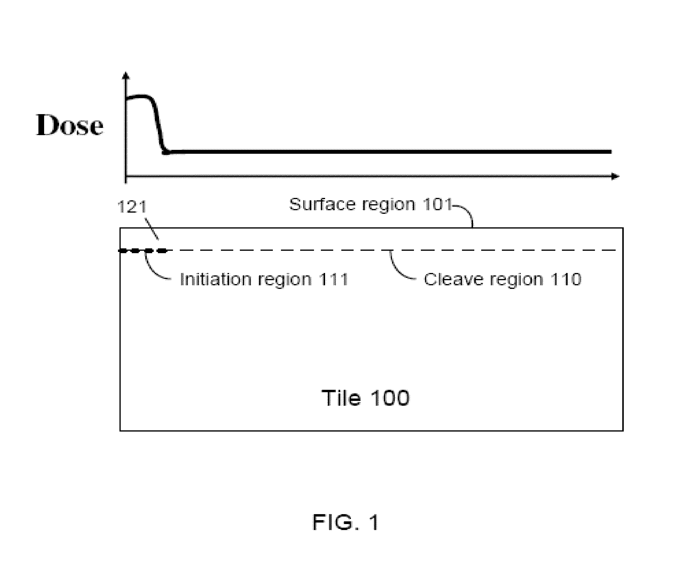
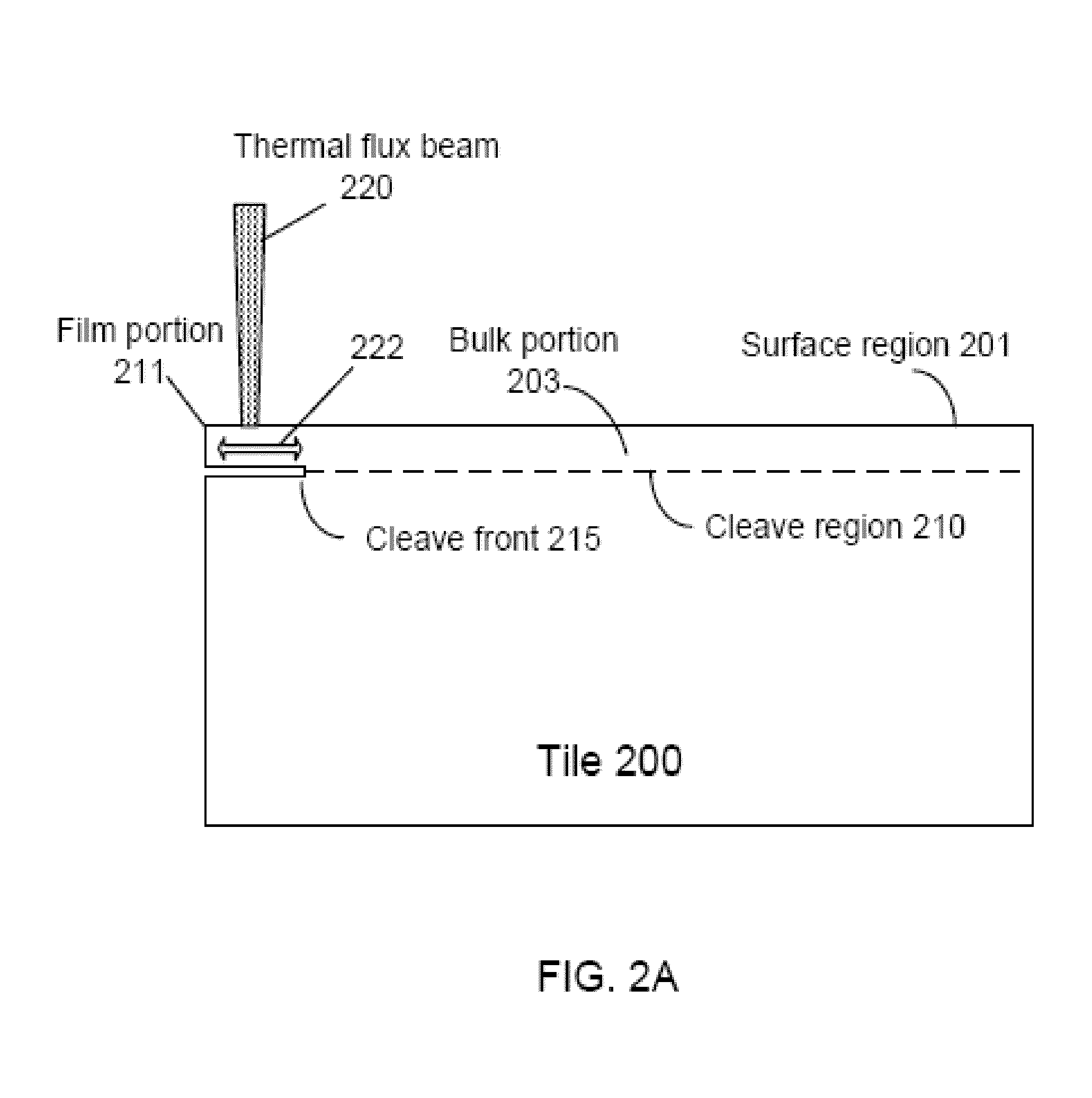
[0028]Particular embodiments of the present invention provide a method and device for layer transfer of films from a tile substrate. Merely by example, it is applied to cleave films along a crystallographic plane of single crystal silicon substrate. But it will be recognized that the invention has a wider range of applicability in both semiconductor and solar industries. For example, other materials such as Germanium, Gallium Arsenide (GaAs), Gallium Nitride (GaN), or Silicon Carbide (SiC) could be subjected to the cleaving process to release films of materials for solar, opto-electronic or semiconductor applications.

[0029]As discussed in background section, the growth of silicon based solar cells relies on driving down a bottleneck for cost in wafering kerf-loss. Traditional sawing, or adopting recently reported wafering technologies (such as multi-wire saw, spark cutting, laser cutting, or plasma cutting) that render thick films suitable for solar cells, may exhibit limited useful...


PUM

PropertyMeasurementUnit
temperatureaaaaaaaaaa
diameteraaaaaaaaaa
temperatureaaaaaaaaaa

Abstract

A method and system for cleaving a film of material utilizing thermal flux. The method includes providing a substrate having a face and an underlying cleave region including a prepared initiation region. Additionally, the method includes subjecting the initiation region to a first thermal flux to form a cleave front separating the cleave region of the substrate to a film portion and a bulk portion. The method further includes subjecting an area of the bulk portion substantially in the vicinity of the cleave front to a second thermal flux to cause a temperature difference above and below the cleave region for inducing a propagation of the cleave front expanding the film portion to the area at the expense of the bulk portion. Furthermore, the method includes determining a scan path for the second thermal flux based on the cleave front. Moreover, the method includes scanning the second thermal flux to follow the scan path to further propagate the cleave front.

Description

CROSS-REFERENCES TO RELATED APPLICATIONS[0001]NOT APPLICABLEBACKGROUND OF THE INVENTION[0002]From the beginning of time, human beings have relied upon the “sun” to derive almost all useful forms of energy. Such energy comes from petroleum, radiant, wood, and various forms of thermal energy. As merely an example, human beings have relied heavily upon petroleum sources such as coal and gas for much of their needs. Unfortunately, such petroleum sources have become depleted and have lead to other problems. As a replacement, in part, solar energy has been proposed to reduce our reliance on petroleum sources. As merely an example, solar energy can be derived from “solar cells” commonly made of silicon.[0003]The silicon solar cell generates electrical power when exposed to solar radiation from the sun. The radiation interacts with atoms of the silicon and forms electrons and holes that migrate to p-doped and n-doped regions in the silicon body and create voltage differentials and an electr...

Claims


Application Information

Patent Timeline
Patent Type & Authority Patents(United States)
IPC IPC(8): H01L21/46H01L21/30
CPCB23K26/365B23K26/361
Inventor HENLEY, FRANCOIS, J.
Owner SILICON GENERAL CORPORATION
Why Eureka
Try Eureka