Arrays of ultrathin silicon solar microcells

a solar cell and array technology, applied in the field of arrays of ultrathin silicon solar cells, can solve the problems of major cost, rate and energy input driver in the production of materials, serious limitations in the industry, and short supply period of electronic-grade si, and achieve convenient transportation and installation characteristics, high efficiency, and low cost. the effect of sacrificing efficiency or performan

Active Publication Date: 2014-03-25
THE BOARD OF TRUSTEES OF THE UNIV OF ILLINOIS
View PDF80 Cites 134 Cited by
  • Summary
  • Abstract
  • Description
  • Claims
  • Application Information

AI Technical Summary

Benefits of technology

[0009]Provided herein are photovoltaics (PV) and related methods for making high efficiency PV that exploit ultrathin solar grade or low grade semiconductors created from bulk semiconductor material, such as Si. In specific embodiments, provided are low-cost PV without unduly sacrificing efficiency or performance. PV of the present invention are optionally lightweight and bendable that provide convenient transportation and installation characteristics. In addition, the PV can be made at least partially optically transparent for use in varied architectural situations such as windows, doors, or skylights. PV systems comprise printable semiconductor-containing structures (e.g., printable semiconductor elements) assembled, organized and / or integrated with other device components, at least in part, via printing-based techniques. Provided herein are systems having performance characteristics and functionality comparable to single crystalline semiconductor based devices fabricated using conventional high temperature processing methods. PV provided herein have device geometries and configurations, such as form factors, component densities, and component positions, accessed by printing that provide a range of useful device functionalities. PV include devices and device arrays exhibiting a range of useful physical and mechanical properties including flexibility, shapeability, conformability and / or stretchablity. PV systems of the present invention include, however, devices and device arrays provided on conventional rigid or semi-rigid substrates, in addition to devices and device arrays provided on flexible, shapeable and / or stretchable substrates.
[0010]This invention also provides PV fabrication and processing steps, methods and materials strategies for making PV systems at least in part via printing techniques, including contact printing, for example using a conformable transfer device, such as an elastomeric transfer device (e.g., elastomer layer or stamp). In specific embodiments, methods of the present invention provide a high-throughput, low cost fabrication platform for making a range of high performance PV systems. Processing provided by the present methods is compatible with large area substrates, such as device substrates for microelectronic devices, arrays and systems, and is useful for fabrication applications requiring patterning of layered materials, such as patterning printable structures and / or thin film layers for electronic and electro-optic devices. Methods of the present invention are complementary to conventional microfabrication and nanofabrication platforms, and can be effectively integrated into existing photolithographic, etching and thin film deposition device patterning strategies, systems and infrastructure. The present PV fabrication methods provide a number of advantages over conventional fabrication platforms including the ability to integrate semiconductor materials having a range of quality, such as ranging from relatively low-quality semiconductor material (e.g., solar grade Si) to high quality semiconductor materials, such as single crystalline semiconductors and semiconductor-based electronic devices / device components, into PV systems provided on large area substrates, polymer device substrates, and substrates having contoured a conformation.
[0011]In an aspect, the present invention provides processing methods using low quality bulk semiconductor wafer starting materials that are processed to provide large yields of printable semiconductor elements with preselected physical dimensions and shapes that may be subsequently transferred, assembled and integrated into solar cells and PV systems via printing. An advantage provided by the present printing-based device fabrication methods is that the printable semiconductor elements retain desirable electronic properties, optical properties and efficiencies compared to conventional PVs even for compositions that use lower quality bulk wafer starting material (e.g., mobility, purity and doping etc.). This can achieve a significant cost reduction in feedstock material, thereby providing low-cost PV. In addition, use of printing-based assembly and integration, for example via contact printing or solution printing, is compatible with device fabrication over large areas, including areas greatly exceeding the dimensions of the bulk wafer starting material and provides control of different mechanical properties (e.g., flexibility, stretchability etc.) that are useful for target applications such as flexible electronics. Further, the present semiconductor processing and device assembly methods provide for very efficient use of the starting semiconductor material for making printable semiconductor elements that can be assembled and integrated into a large number of devices or device components. This aspect of the present invention is advantageous because very little of the semiconductor wafer starting material is wasted or discarded during processing, thereby providing a processing platform capable of low cost fabrication of PV systems. In an aspect, the invention is described in terms of the percentage by weight of the Si wafer feedstock that is used in making the PV, such as greater than 50%, greater than 60% or greater than 90% of the Si wafer starting material is transferred to the solar cell substrate.

Problems solved by technology

However, periodic shortages of electronic-grade Si represent a serious limitation to the industry.
Furthermore the extreme high purity required of Si used in these devices presents major cost, rate, and energy input driver in production of the material.
Shortage of Si feedstock contributes to high cost related to solar power generation and, accordingly, much effort has been devoted to research and development into thin film solar cells.
However, Cd toxicity and ultimately Te mineral resource limitations may prevent this technology from growing beyond a moderate level.
Presently, silicon PV technology has high materials costs, due to the relatively inefficient use of the bulk silicon material.
In addition, these modules are rigid and heavy, both of which are negatives from the consumer standpoint.
Reviews of amorphous and crystalline thin-film Si solar cell activities suggest that near term prospects for significant improvements in thin film amorphous Si cell efficiencies and stability are unlikely without an unexpected breakthrough, thus limiting producers to low margin, highly competitive market applications.
As the market continues to grow from megawatt to gigawatt scale, however, such thick devices are expected to lose this cost advantage and thin film devices will become the logical choice.
This product is undergoing rapid scale-up and may ultimately exceed the production volume of c-Si.
While early successes demonstrated near state-of-the-art thin film Si cell efficiencies, which were stable for long periods of time, the ultimate potential of crystalline thin film Si technologies remains less clear due to their higher processing cost and slower throughput when compared to amorphous Si.
Unlike crystalline thin film Si, analysis has shown that the cost structure of CdTe and CIGS can be favorable but that issues related to material availability, low efficiency, and Environmental, Health, and Safety present considerable market risk.
Third, current embodiments of SLIVER modules are not mechanically flexible, and they cannot readily incorporate other key technologies, such as molded low concentration micro-optics, and printed interconnects.

Method used


Image

  • Arrays of ultrathin silicon solar microcells
  • Arrays of ultrathin silicon solar microcells
  • Arrays of ultrathin silicon solar microcells

Examples


example 1

Ultra Thin Flexible Solar (UTFS) Devices and Methods

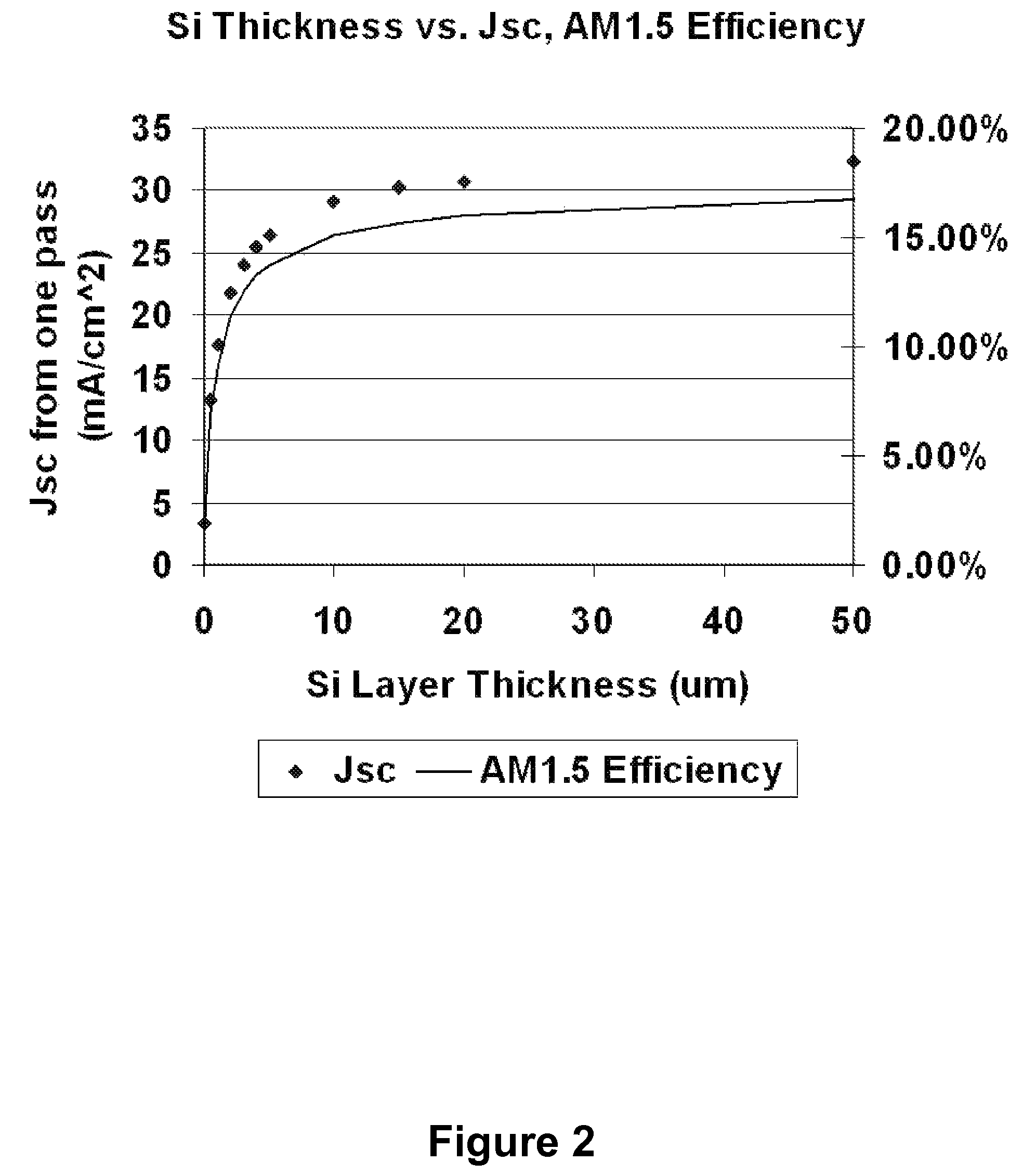
[0097]There is currently interest in thin-film PV technologies, since these systems have the potential for lower cost (due to less active material usage), and also have the ability to be deposited onto polymer substrates for low weight and flexibility. Presently, investigation is ongoing in thin film materials such as amorphous silicon, cadmium telluride (CdTe) and copper indium gallium diselenide (CIGS). CIGS-based PV cells have demonstrated cell efficiencies of 19.2%, the highest of any polycrystalline thin film material. These cells are small, laboratory-scale devices; to date, the highest large-area flexible module efficiencies are on the order of 10%. Cheaper thin film semiconductors enable material cost savings, but induce higher processing costs as the cells need to be fabricated / processed on large area substrates. Also, only low / moderate temperature processes can be used on the final assembly substrate

[0098]Ideally, one wou...

example 2

Arrays of Monocrystalline Silicon Solar Microcells for Modules With Ultra-thin, Mechanically Flexible, Semi-transparent and Micro-optic Concentrator Designs

[0124]Silicon, in amorphous or various crystalline forms, is used in >90% of all installed photovoltaic (PV) capacity. The high natural abundance of silicon, together with the excellent reliability and good efficiency of solar cells made with it suggest its continued use, on massive scales, for the foreseeable future. As a result, although there is significant promise for organics, nanocrystals, nanowires and other new materials for photovoltaics, many opportunities continue to exist for research into unconventional means for exploiting silicon in advanced PV systems. This example describes modules that use large scale arrays of silicon solar micro-cells (μ-cells) created from bulk wafers and integrated in diverse spatial layouts on foreign substrates by transfer printing. The resulting devices can offer useful features, includin...

example 3

Fabrication of Si Microbar Cells (μb-cells)

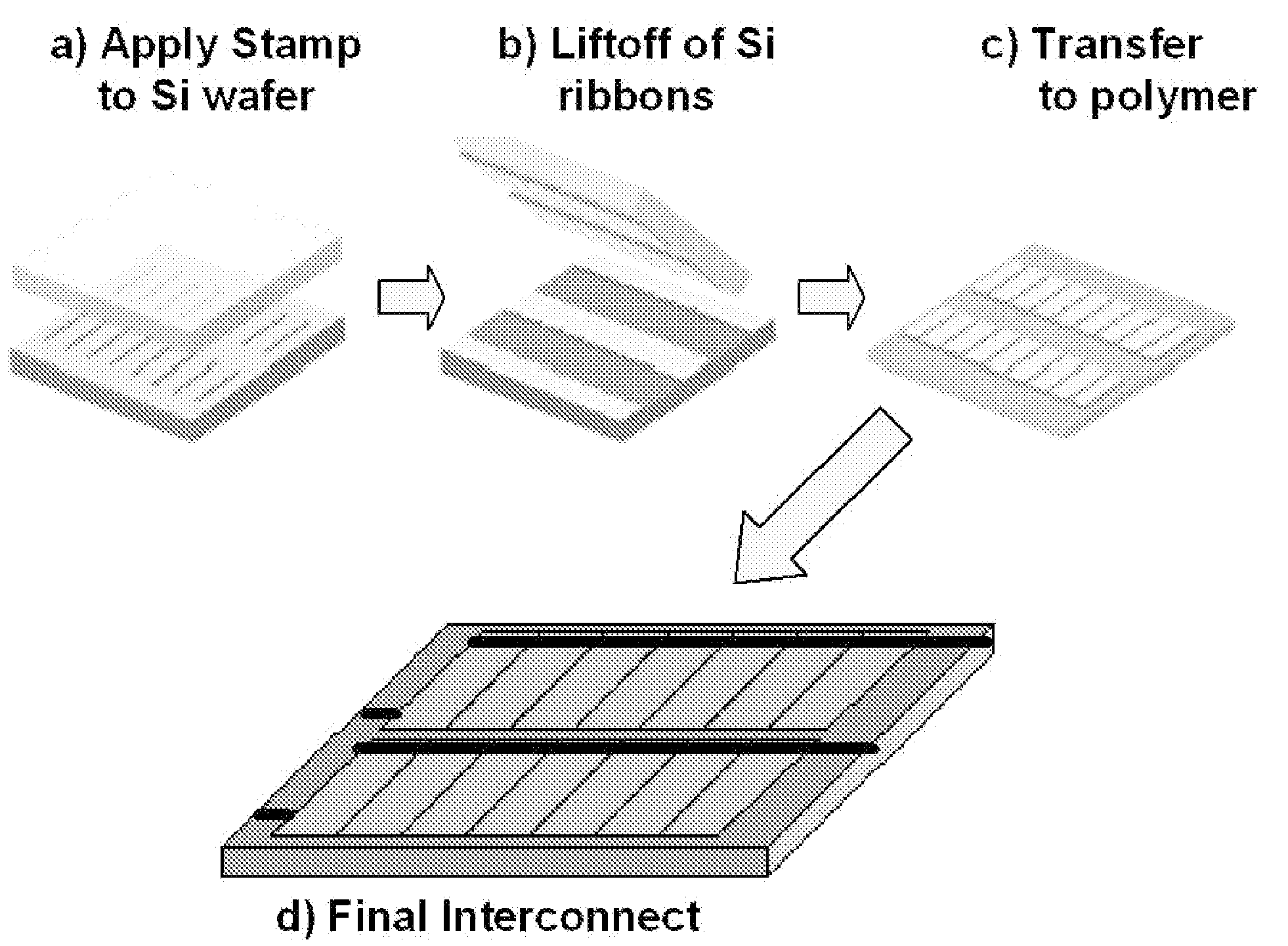
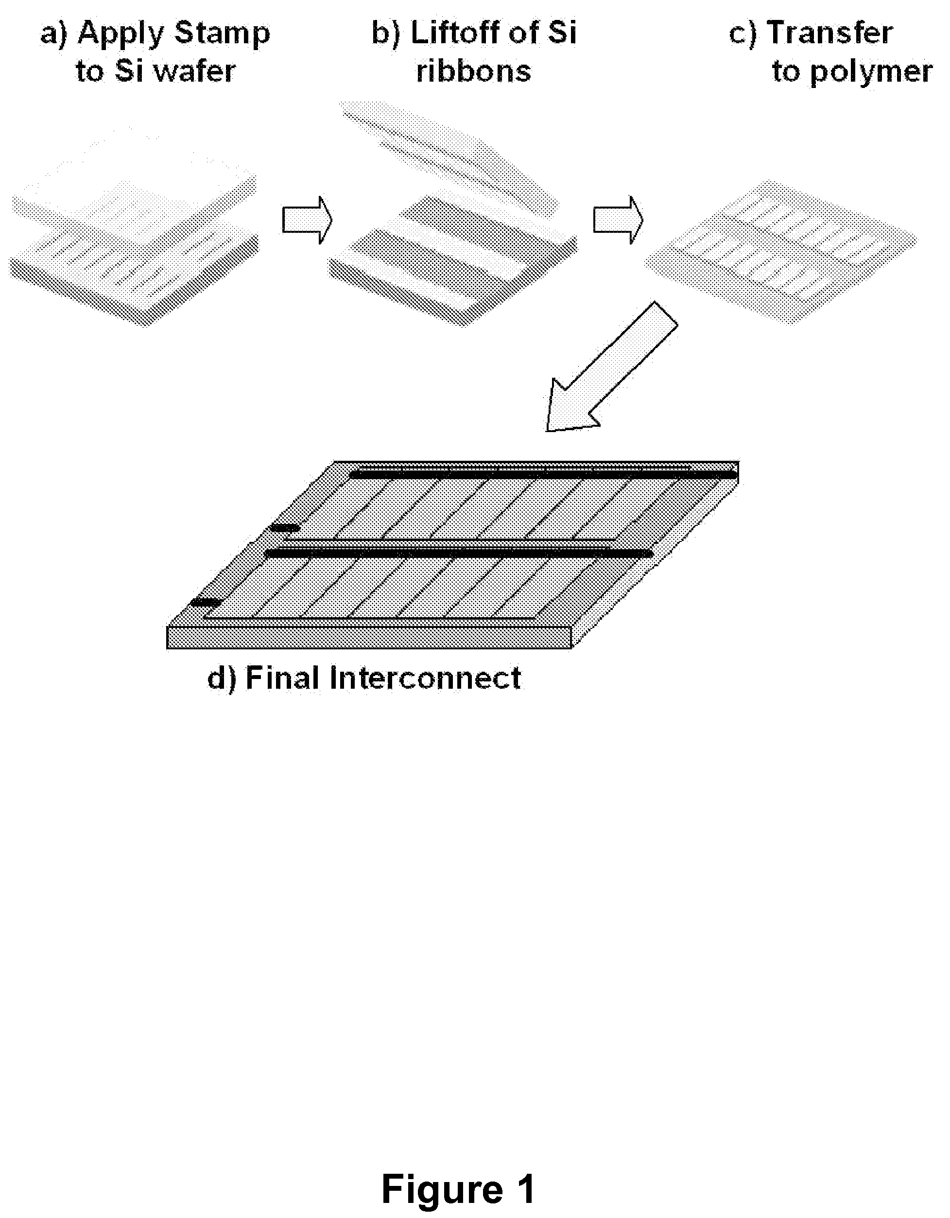
[0204]An anisotropic wet etching process provides a simple means to create ultrathin, monocrystalline Si cells from bulk wafers of material. FIG. 30 shows the process for forming the thin Si[11,12], which begins with patterning of lines of resist on the surface of a (111) Si wafer. (Published data indicate no differences in efficiency for conventional cells made with (111) compared to (100) Si.[35,36]) A vertical trench etch followed by an anisotropic undercut etch (e.g. tetramethyl ammonium hydroxide, which etches along the direction ˜50× faster than other directions) yields bars or ribbons of Si that remain attached to the underlying wafer only at their ends. The vertical etch defines the thicknesses of the bars / ribbons; the patterning step defines the lengths, widths and spacings.

[0205]In this process, the etching procedures for the vertical trenches and undercuts yield structures that utilize up to 85% of the available Si. Doping techn...


PUM


Abstract

Provided are solar cells, photovoltaics and related methods for making solar cells, wherein the solar cell is made of ultrathin solar grade or low quality silicon. In an aspect, the invention is a method of making a solar cell by providing a solar cell substrate having a receiving surface and assembling a printable semiconductor element on the receiving surface of the substrate via contact printing. The semiconductor element has a thickness that is less than or equal to 100 μm and, for example, is made from low grade Si.

Description

CROSS-REFERENCE TO RELATED APPLICATIONS[0001]This application is a national stage application under 35 U.S.C. §371 of PCT / US2009 / 058231, filed Sep. 24, 2009, which claims the benefit of priority of U.S. Provisional Patent Application No. 61 / 099,801 filed Sep. 24, 2008, which are hereby incorporated by reference in their entirety to the extent not inconsistent herewith.STATEMENT REGARDING FEDERALLY SPONSORED RESEARCH OR DEVELOPMENT[0002]This invention was made at least in part with government support under DE-FG02-07ER46453 and DE-FG02-07ER46471 awarded by the U.S. Department of Energy and DMI-0328162 awarded by the National Science Foundation. The government has certain rights in the invention.BACKGROUND OF THE INVENTION[0003]Photovoltaic solar cells convert sunlight directly into electrical energy. Silicon is the dominant material for photovoltaic (PV) solar cells, with over 90% of all solar cells being made from crystalline and polycrystalline Si. In fact, the share of cells made ...

Claims


Application Information

Patent Timeline
Patent Type & Authority Patents(United States)
IPC IPC(8): H01L31/18
CPCH01L31/035281Y02E10/547H01L31/028H01L31/1896H01L31/0508H01L31/1804H01L31/048Y02P70/50H01L31/18
Inventor ROGERS, JOHN A.ROCKETT, ANGUS A.NUZZO, RALPHYOON, JONGSEUNGBACA, ALFRED
Owner THE BOARD OF TRUSTEES OF THE UNIV OF ILLINOIS
Why Eureka
Try Eureka