Eureka AIR delivers breakthrough ideas for toughest innovation challenges, trusted by R&D personnel around the world.

Compositions and methods for the selective removal of silicon nitride

a silicon nitride and selective etching technology, applied in silicon compounds, instruments, photomechanical apparatuses, etc., can solve the problems of increased parasitic capacitance, tight tolerance of pattern definition, device contact resistance, etc., to achieve high selectiveness, high etch rate, and effective and efficient etching of a layer

Active Publication Date: 2014-07-15
ENTEGRIS INC
View PDF34 Cites 24 Cited by
  • Summary
  • Abstract
  • Description
  • Claims
  • Application Information

AI Technical Summary

Benefits of technology

[0012]The present invention relates to a removal composition and process for selectively etching silicon nitride in the presence of silicon oxide, polysilicon and / or metal silicides, and more particularly to a composition and process for effectively and efficiently etching a layer of silicon nitride at a high etch rate and with high selectivity with respect to exposed or underlying layers of silicon oxide, polysilicon and / or metal silicides, particularly in a multilayer semiconductor wafer structure.

Problems solved by technology

Such requirements however cause problems of increased parasitic capacitance, device contact resistance (gate, source and drain contacts in MOSFET devices), and tight tolerance of pattern definition.
For very small sub-micron or sub-half-micron or even sub-quarter-micron modern silicon devices, the conventional photolithographic technique for patterning contacts will not meet the required tolerance of critical dimensions.
One problem encountered during the formation of self-aligned gate structures has been the selective removal of silicon nitride materials relative to polysilicon, silicon oxide and / or metal silicide materials.
For example, during the anisotropic etching of the silicon nitride layer covering the gate electrodes, the underlying silicon oxide layer and silicon substrate are often damaged as well, causing a deteriorated reliability of a semiconductor device.
Disadvantages associated with the use of hot phosphoric acid etches include the corrosion of metal silicide materials, e.g., gate contact materials, the etching of silicon oxide, and process control due to the difficulty associated with maintaining a specific amount of water in the process solution.
In addition, hot phosphoric acid has been a difficult medium to adapt to single wafer tools, which have become increasingly preferred by many manufacturers.
A Si3N4:SiO2 selectivity of about 10:1 can be achieved through dilution, however, the etch rate of silicon nitride is compromised or above-ambient pressure must be used.
Still another process to remove silicon nitride includes the dry etch removal using halogenated gaseous species, however, the Si3N4:SiO2 selectivity ratio is even worse than that obtained using the aforementioned wet etch processes.

Method used


Image

  • Compositions and methods for the selective removal of silicon nitride
  • Compositions and methods for the selective removal of silicon nitride
  • Compositions and methods for the selective removal of silicon nitride

Examples


example 1

[0077]Concentrated formulations were made by combining 15 g fluorosilicic acid, 35 g of DPGME or diethylene glycol methyl ether and 1.52-1.92 g of TEOS or an equivalent amount of 1 micron silica glass powder. The concentrate including TEOS as the silicic acid source is aged by stirring at 20-23° C. for at least 1 hour and then diluted for use as the removal composition of the invention. The concentrate including silica powder is stirred for 1-3 days at room temperature and then diluted for use as the removal composition of the invention. For example, the concentrate may be diluted with deionized water in a 10:1 DI water to concentrate ratio.

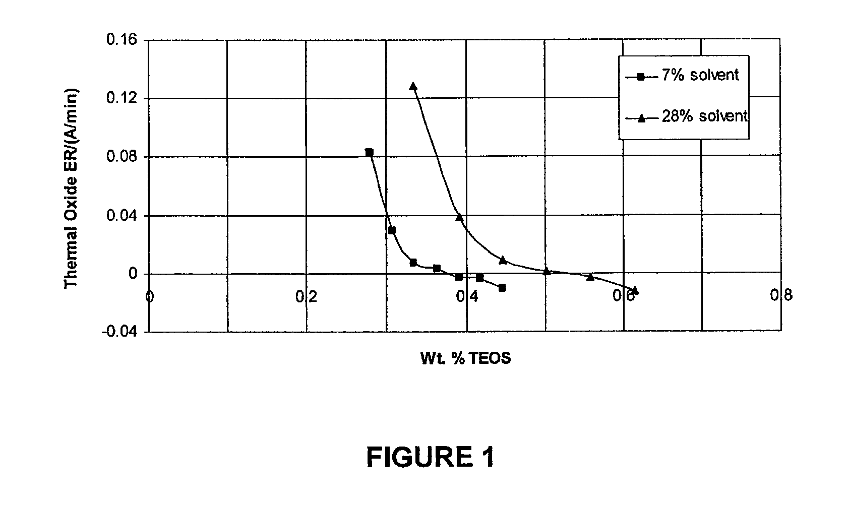
[0078]Typical etch rates for RTCVD-deposited silicon nitride using removal compositions such as this are in the range of about 7 to about 16 Å min−1 at 82-86° C. When TEOS is the silicic acid source, no etching of thermal silicon oxide was detected after 15-22 hours at 85° C. (experimental error is about 1-5 Å).

example 2

[0079]Blanketed RTCVD-deposited Si3N4 (˜850 Å thick) was immersed in Formulations A and B at 80° C. for up to 100 min. The wafers were first measured using an optical interferometer (Nanospec) to determine the pre-immersion thickness, followed by individually immersing each wafer in clean removal composition, pulling the wafers in 25 minute intervals, rinsing with deionized water, blowing dry with nitrogen and post-immersion measuring using the optical interferometer to determine the change in thickness to derive the etch rate of silicon nitride. The results are tabulated in Table 1.

[0080]

TABLE 1Etch rate of Silicon Nitride in Formulations A and B.Pre-Post-Etch rate / ÅFormulationTime / minimmersion / Åimmersion / Åmin−1A25843.1525.97512.685A50841.475229.47512.240A75837.77583.410.058A100841.67591.97.498B25838.7598.99.592B50844.075344.59.991B75842.85151.19.223B100843.62584.457.592

[0081]It can be seen that the silicon nitride was completely removed using formulations A and B in about 75 minut...

example 3

[0085]Blanketed RTCVD-deposited Si3N4 (˜600 Å thick) was immersed in Formulations B, C, and E at 80° C. for 30 min. The wafers were first measured using an optical interferometer (Nanospec) to determine the pre-immersion thickness, followed by individually immersing each wafer in clean removal composition, pulling the wafers, rinsing with deionized water, blowing dry with nitrogen and post-immersion measuring using the optical interferometer to determine the change in thickness to derive the etch rate of silicon nitride. The results are tabulated in Table 3.

[0086]

TABLE 3Etch rate of Silicon Nitride in Formulations B, C and E.Pre-Post-Etch rate / ÅFormulationimmersion / Åimmersion / Åmin−1C595.95338.488.58E579.78337.708.07B627.35391.357.87B609.85354.108.53B616.20374.728.05

[0087]In addition, blanketed NiPtSi was immersed in the same formulations at 80° C. for 30 minutes and the pre-immersion and post-immersion sheet resistance measured using a four-point probe. The results are tabulated in ...


PUM

PropertyMeasurementUnit
diameteraaaaaaaaaa
wt. %aaaaaaaaaa
wt. %aaaaaaaaaa

Abstract

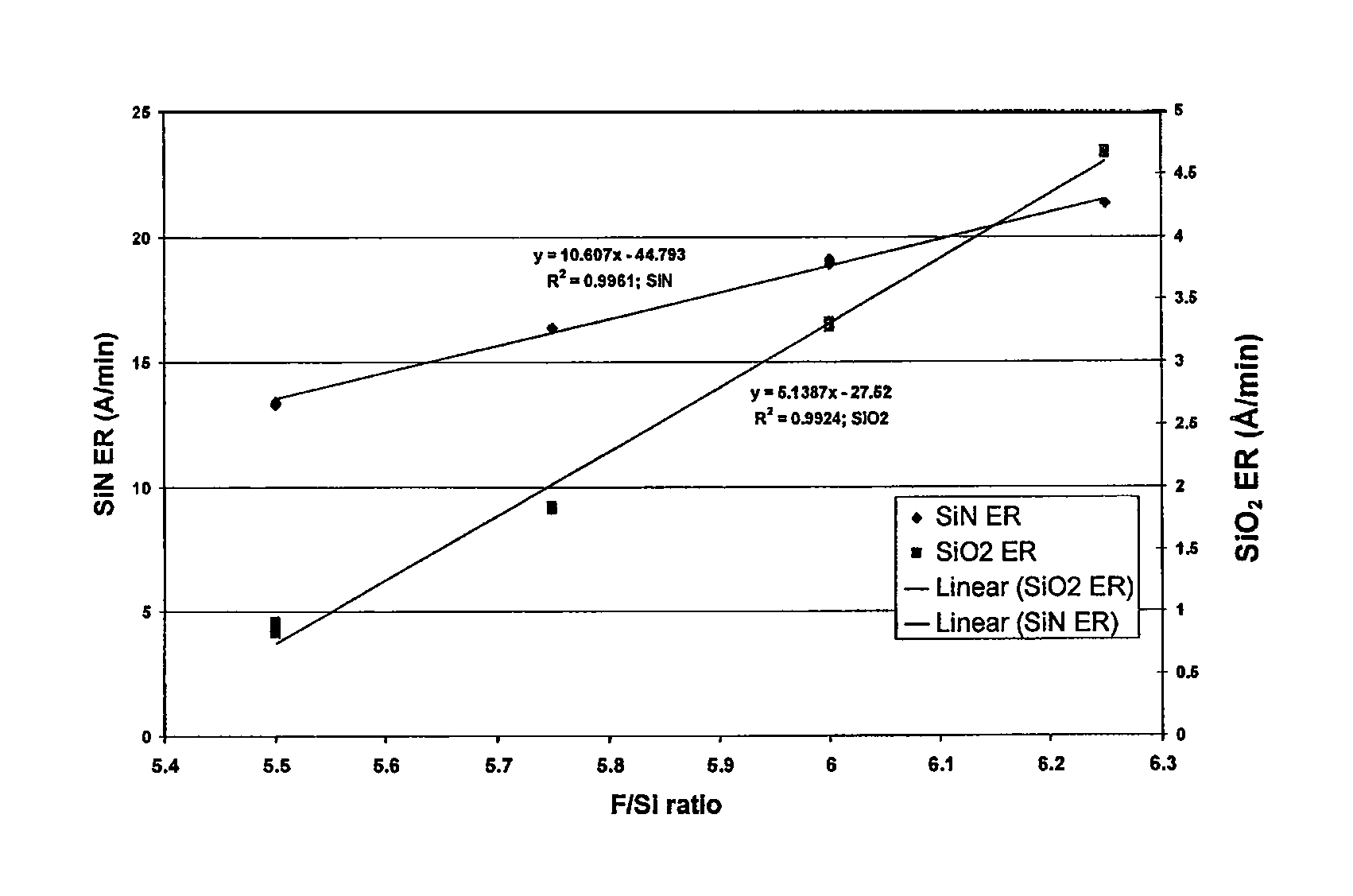
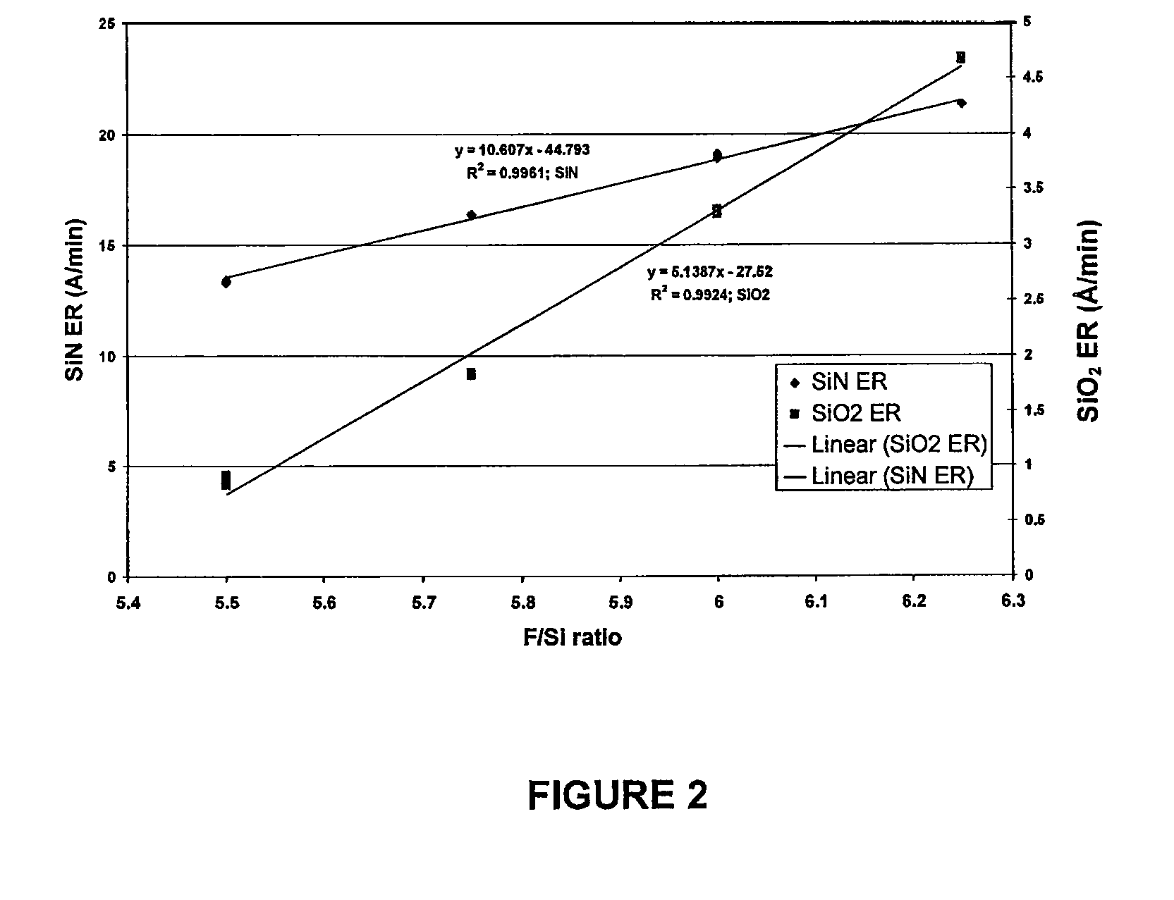
Compositions useful for the selective removal of silicon nitride materials relative to poly-silicon, silicon oxide materials and / or silicide materials from a microelectronic device having same thereon. The removal compositions include fluorosilicic acid, silicic acid, and at least one organic solvent. Typical process temperatures are less than about 100° C. and typical selectivity for nitride versus oxide etch is about 200:1 to about 2000:1. Under typical process conditions, nickel-based silicides as well as titanium and tantalum nitrides are largely unaffected, and polysilicon etch rates are less than about 1 Å min−1.

Description

CROSS-REFERENCE TO RELATED APPLICATIONS[0001]This application is filed under the provisions of 35 U.S.C. §371 and claims the priority of International Patent Application No. PCT / US07 / 88643 filed on 21 Dec. 2007 and entitled “Compositions and Methods for the Selective Removal of Silicon Nitride” which claims priority to U.S. Provisional Patent Application No. 60 / 871,391 filed on 21 Dec. 2006, both of which are hereby incorporated herein by reference in their entirety.FIELD OF THE INVENTION[0002]The present invention relates to a composition and process for selectively etching silicon nitride in the presence of silicon oxide, polysilicon and / or metal silicides, and more particularly to a composition and process for effectively and efficiently etching a layer of silicon nitride at a high etch rate and with high selectivity with respect to exposed or underlying layers of silicon oxide, polysilicon and / or metal silicides, particularly in a multilayer semiconductor wafer structure.DESCRIP...

Claims


Application Information

Patent Timeline
Patent Type & Authority Patents(United States)
IPC IPC(8): C09K13/08C03C15/00C09K13/00C03C25/68C09K13/04C09K13/06
CPCH01L21/31111G03F7/422H01L2924/0002C09K13/08B65D85/70H01L21/0206
Inventor COOPER, EMANUEL I.SPARKS, EILEEN R.BOWERS, WILLIAM R.BISCOTTO, MARK A.YANDERS, KEVIN P.KORZENSKI, MICHAEL B.SONTHALIA, PRERNATHOMAS, NICOLE E.
Owner ENTEGRIS INC
Why Eureka
Eureka Blog
Learn More