Room-temperature magnetoelectric multiferroic thin films and applications thereof

a magnetoelectric multiferroic, thin film technology, applied in the field of room-temperature magnetoelectric multiferroic thin film and applications thereof, can solve the problems of high leakage, low me voltage coefficient, and unsuitable application of weak field sensor, and achieve well behaved and saturated c(v) hysteresis, the effect of low leakag

Active Publication Date: 2014-08-12
UNIVERSITY OF PUERTO RICO
View PDF0 Cites 14 Cited by
  • Summary
  • Abstract
  • Description
  • Claims
  • Application Information

AI Technical Summary

Benefits of technology

[0018]According to a further aspect of the invention, a MMIS device structure of Pt(PFWx−PZT1-x) / SrTiO3 / Si (111) is provided, fabricated for different compositions of (PFWx−PZT1-x) (x=0.20≦x≦0.60), showing well behaved and saturated C(V) hysteresis with 3-4 V memory windows, and low leakage and serving as excellent candidates for non-volatile memory applications and multiferroic RAMs.

Problems solved by technology

In this case practical devices favor sandwich-type bilayer or multilayer composites of ferroelectrics such as lead zirconate-titanate (PZT) with magnets such as terphenyl-d but this configuration yields low ME voltage coefficients which is not suitable for weak field sensor applications.
Moreover, they operate only at cryogenic temperatures.
0.03 emu / cc), high leakage current, and it does not permit switching of neither magnetization with electric fields nor polarizations with magnetic fields.

Method used


Image

  • Room-temperature magnetoelectric multiferroic thin films and applications thereof
  • Room-temperature magnetoelectric multiferroic thin films and applications thereof
  • Room-temperature magnetoelectric multiferroic thin films and applications thereof

Examples


example 1

Preparation and Properties of (PFWx-PZT1-x) (0.20≦x≦0.40) by Chemical Solution Method

Materials and Methods

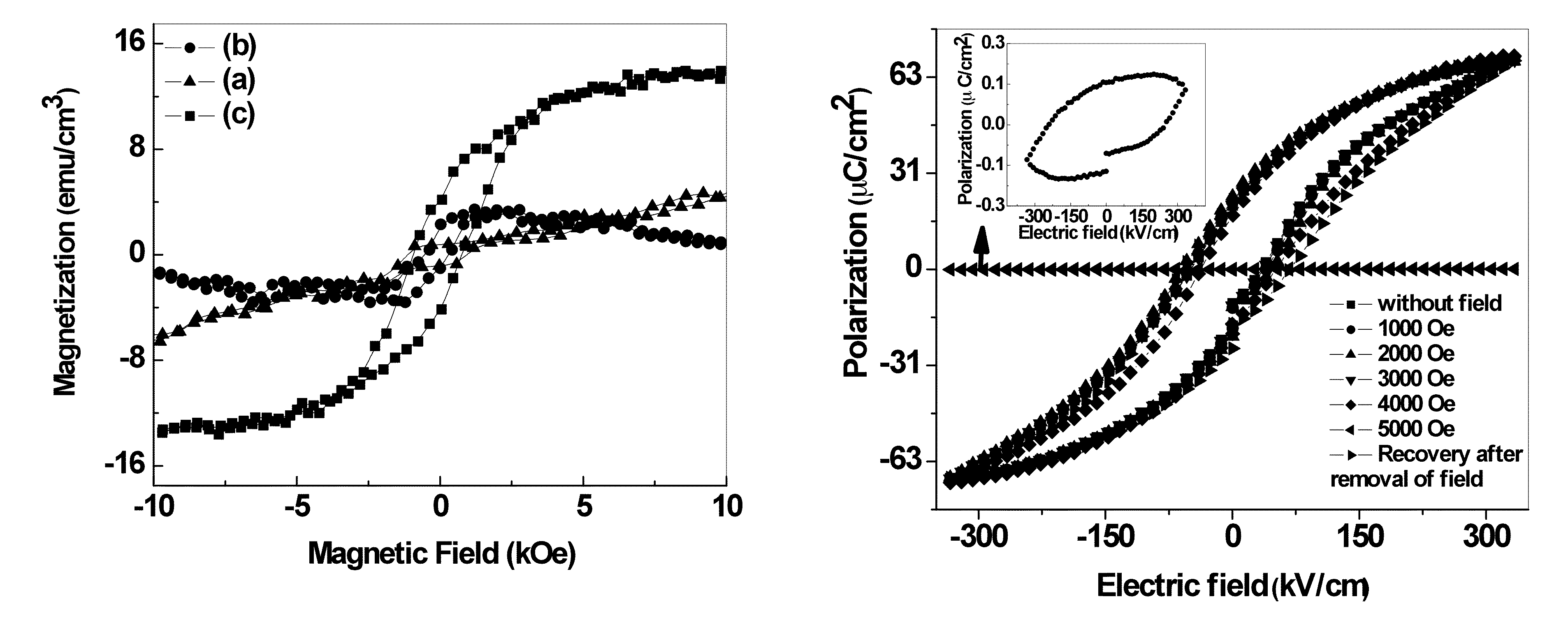
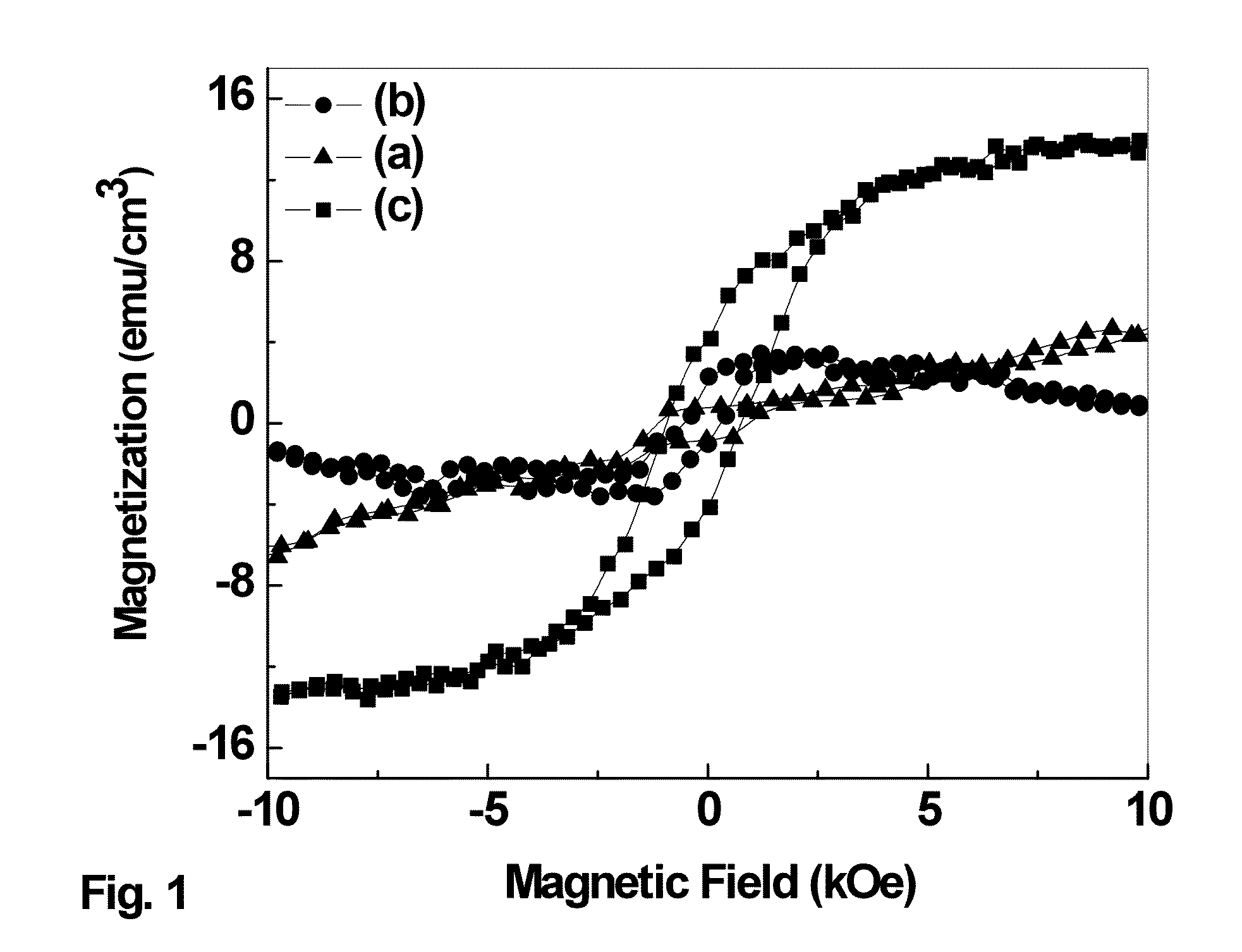
[0050]Ferroelectric (PFWx−PZT1-x) (0.20≦x≦0.40) thin films were deposited on Pt / TiO2 / SiO2 / Si(100) substrates using chemical solution deposition (CSD). The high purity (>99.9%) precursor materials (i.e., lead acetate trihydrate, iron 2-4 pentanedieonate, titanium isopropoxide, zirconium isopropoxide and tungsten isopropoxide) were bought from Alfa Aesar and used for making stock solutions. For good quality films a (PFWx−PZT1-x) (0.20≦x≦0.40) solution of 0.2-0.3 molar concentration was spin coated at 3000 rpm for 30 seconds and pyrolyzed at 673 K for 2 minutes. This process was repeated several times in order to get desired film thickness. Rapid thermal annealing (RTA) was performed at different temperatures from 873 K-1023 K for different time intervals ˜60-300 seconds to get the desired phase and high density. The substrate consists of a layer of Si (about 350 μm thick), SiO2 (a...

example 2

Preparation and Properties of (PFWx−PZT1-x) (0.20≦x≦0.80) by Pulsed Laser Method

Materials and Methods

[0061]Stoichiometric ceramic targets of (PFWx−PZT1-x)(0.20≦x≦0.80) with 10% excess of lead oxide (to compensate for loss of volatile Pb) were synthesized by a conventional solid-state route. Three different compositions of (PFWx−PZT1-x) films with varying deposition temperature were fabricated by pulsed laser deposition (PLD) employing a KrF excimer laser (A=240 nm). The conducting La0.67Sr0.33CoO3 (LSCO) layer was grown on MgO (100) substrate at 873 K under an oxygen pressure of 300 mTorr, using a laser energy density of (1.8 J / cm2) and repetition rate of 10 Hz, followed by normal cooling in oxygen atmosphere. LSCO was used as bottom electrode for all kind of electrical measurements. The (PFWx−PZT1-x) layer was then deposited on the LSCO layer at 873 K under an oxygen pressure of 200 mTorr, using a laser energy density of (1.5 J / cm2) and repetition rate of 10 Hz. After deposition, (...

example 3

Fabrication of MMIS Device Structure of (PFWx−PZT1-x) (0.20≦x≦0.40) on p-Type Silicon

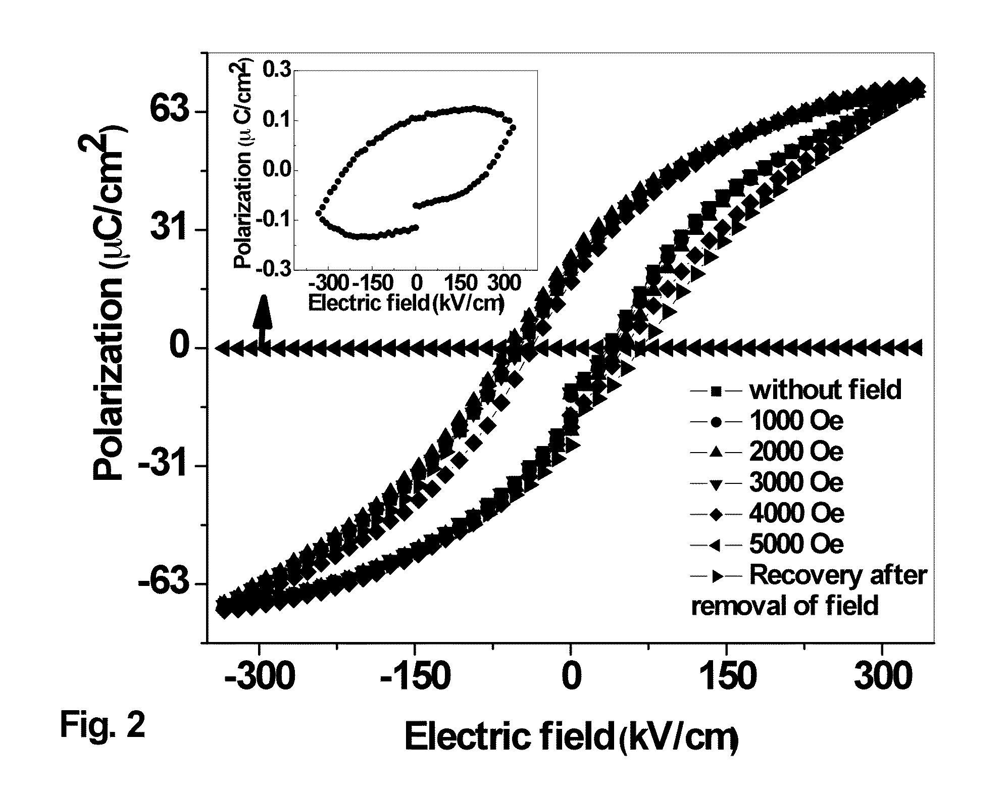
[0069]Materials and Methods:

[0070]To fabricate the MMIS structure, 6 nm SrTiO3 (ST) was deposited on a p-type Si(111) substrate by PLD technique. Attempts at fabrication of the structure by depositing amorphous SrTiO3 at low temperatures yielded much higher leakage currents, in turn giving unsaturated accumulation regions under the application of negative bias voltage. So instead crystalline SrTiO3 (6 nm) was grown at 973 K with 100 mTorr of oxygen atmosphere. Three different compositions of (PFWx−PZT1-x) films with varying deposition temperature were fabricated by PLD employing a KrF excimer laser (λ=240 nm). The (PFWx−PZT1-x) layer was then deposited on the ST layer at 600° C. under an oxygen pressure of 200 mTorr, using a laser energy density of (1.5 J / cm2) and repetition rate of 10 Hz. After deposition the (PFWx−PZT1-x) was annealed at 873 K for 30 minutes in oxygen at a pressure of 300 Torr. Fi...


PUM

PropertyMeasurementUnit
temperatureaaaaaaaaaa
dielectric constantaaaaaaaaaa
temperatureaaaaaaaaaa

Abstract

The invention provides a novel class of room-temperature, single-phase, magnetoelectric multiferroic (PbFe0.67W0.33O3)x (PbZr0.53Ti0.47O3)1-x (0.2≦x≦0.8) (PFWx−PZT1-x) thin films that exhibit high dielectric constants, high polarization, weak saturation magnetization, broad dielectric temperature peak, high-frequency dispersion, low dielectric loss and low leakage current. These properties render them to be suitable candidates for room-temperature multiferroic devices. Methods of preparation are also provided.

Description

GOVERNMENT INTEREST[0001]The claimed invention was made with U.S. Government support under grant numbers W911NF-05-1-0340, W911NF-06-1-0030, and W911NF-06-1-0183 awarded by the Department of Defense (DOD) and grant number FG 02-08ER46526 awarded by the Department of Energy (DoE). The government has certain rights in this invention.BACKGROUND OF THE INVENTION[0002]The development of practical magnetoelectric (ME) multiferroic devices for industry is concentrated on two embodiments: The first is for weak-field sensors for applications such as mine detection in harbors or related military devices. In this case practical devices favor sandwich-type bilayer or multilayer composites of ferroelectrics such as lead zirconate-titanate (PZT) with magnets such as terphenyl-d but this configuration yields low ME voltage coefficients which is not suitable for weak field sensor applications. The second is for random access memory elements where the ability to switch magnetization with applied ele...

Claims


Application Information

Patent Timeline
Patent Type & Authority Patents(United States)
IPC IPC(8): H01L29/82
CPCG11C11/22H01L29/784H01L41/16H01L41/318H01L29/516H01L41/316H10N30/85H10N30/076H10N30/078
Inventor KATIYAR, RAM SKUMAR, ASHOKSCOTT, JAMES F
Owner UNIVERSITY OF PUERTO RICO
Why Eureka
Try Eureka