
Forming active channel regions using enhanced drop-cast printing

a technology of active channel region and drop-cast printing, which is applied in the direction of electroluminescent light sources, thermoelectric devices, electric lighting sources, etc., can solve the problems of difficult to grow organic single crystals in the highest mobility direction of difficult to grow organic single crystals in active channel region in transistors, and conventional inkjet printing techniques are unable to provide well-oriented organic crystals in active channel regions. , the effect of good electrical properties

Active Publication Date: 2014-10-14
SEOUL NAT UNIV R&DB FOUND
View PDF10 Cites 5 Cited by
  • Summary
  • Abstract
  • Description
  • Claims
  • Application Information

AI Technical Summary

Benefits of technology

The patent describes a method for making electrical components using organic semiconductors. The method involves dropping a liquid containing these semiconductors onto a substrate, which is then heated to cause the organics to evaporate. The evaporation causes the organics to crystallize, resulting in well-oriented crystals. This method produces better quality components than traditional inkjet printing, leading to improved electrical properties.

Problems solved by technology

However, growing crystals in the highest-mobility direction on an active channel region in OFETs is technically a significant challenge (Z. Bao, et al., Nature 2006, 444, 913).
Moreover, in solution-based processes, which are generally favorable for isotropic growth of crystals, it is very difficult to grow a well-oriented organic single crystal in an active channel region in transistors (T. Yamao, et al., Chem. Mater. 2007 19, 3748).
However, conventional inkjet printing techniques are unable to provide well-oriented organic crystals for an active channel region in OFETs.
As a result, carrier mobility is not satisfactory, and thus the OFETs may not be suitable for practical applications.

Method used


Image

  • Forming active channel regions using enhanced drop-cast printing
  • Forming active channel regions using enhanced drop-cast printing
  • Forming active channel regions using enhanced drop-cast printing

Examples


first embodiment

[0034]A number of solution-processable organic semiconductor materials have been synthesized, characterized, and fabricated as organic transistors (S. Allard, Angew. Chem. Int. Ed. 2008, 47, 4070).

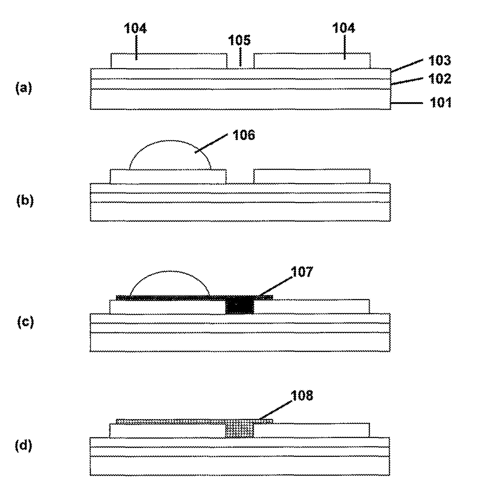
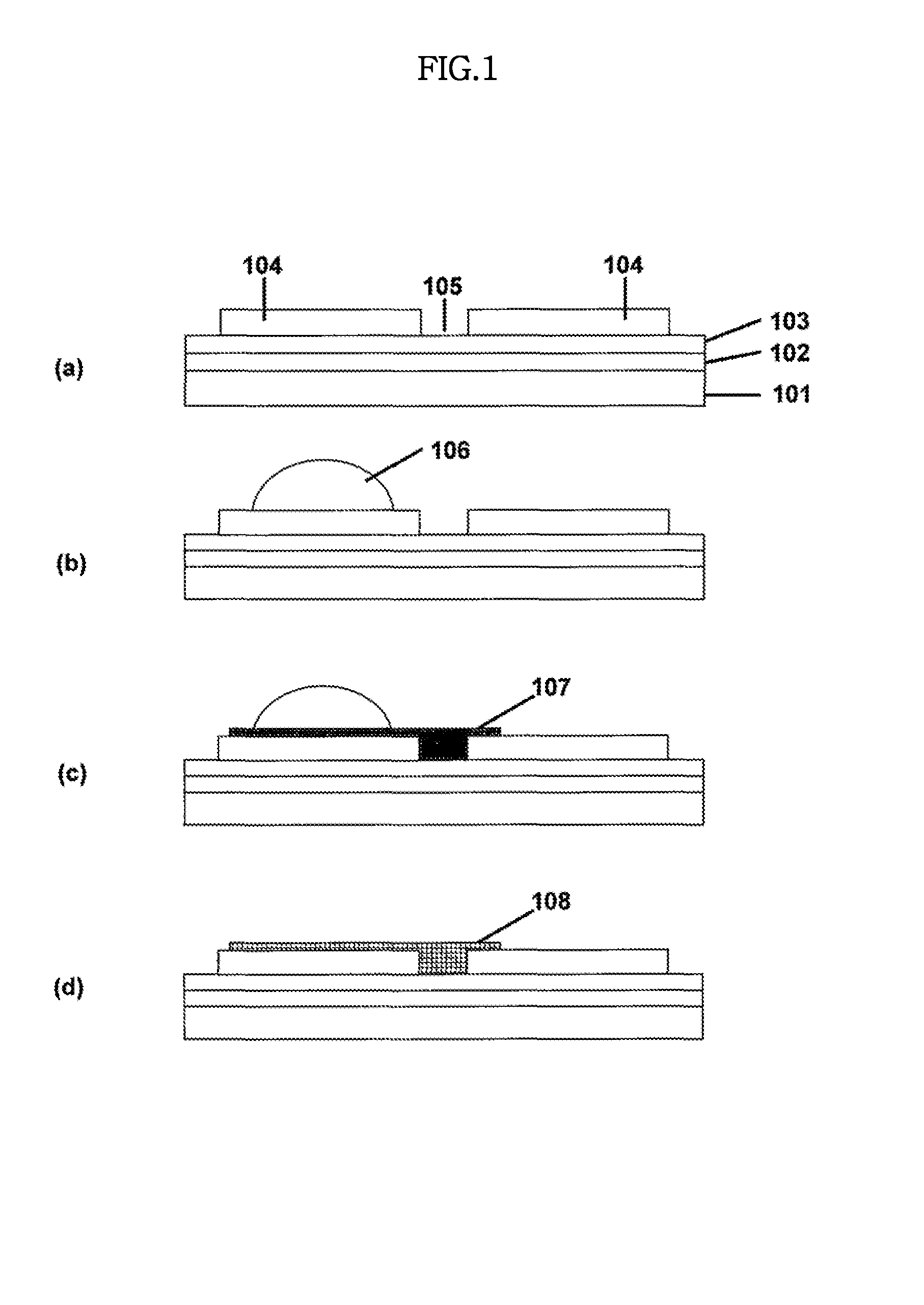
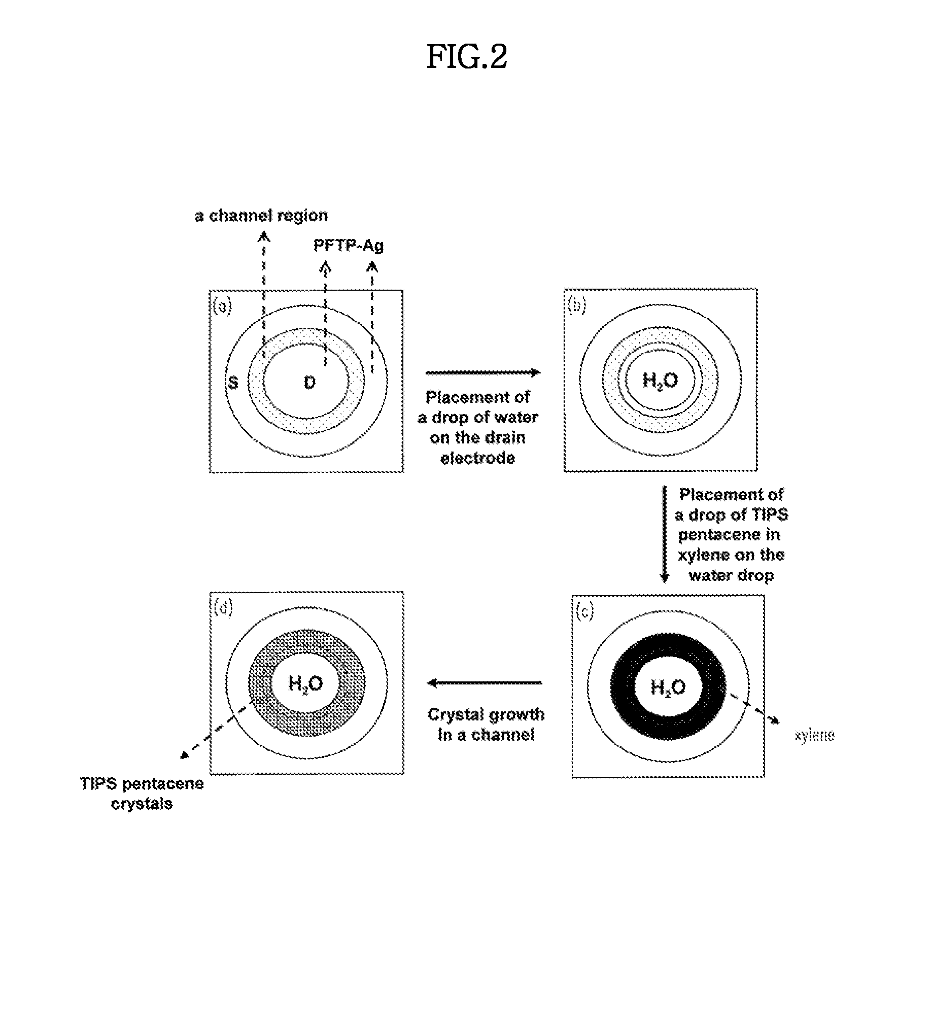
[0035]Among them, a TIPS pentacene has been widely used to fabricate high-performance OTFTs, as it has high solubility in most organic solvents and has a high degree of π-overlap that contribute to the high charge-carrier mobility of OFETs (J. E. Anthony, Angew. Chem. Int. Ed. 2008, 47, 452). In the present exemplary embodiments, to form well-oriented TIPS pentacene crystals on an active channel region in bottom-contact OFETs, the evaporation rates of xylene solvent were appropriately controlled through its interaction with polar H2O.

[0036]FIG. 2 is a schematic illustration of an example of the present method using a two-liquid system. It shows the direct growth of well-oriented TIPS pentacene crystals on an active channel region in bottom-contact OFETs. Dozens of TIPS pentacene crystals a...

second embodiment

[0044]FIG. 7 shows the polarized optical micrograph of the TIPS pentacene transistors fabricated by a conventional drop-casting printing method, whereby bottom-contact electrodes were used and a drop(s) of o-xylene solution (˜0.03 μl) containing TIPS pentacenes (0.8 wt %) was placed onto the top of an active channel region using a micropipette. The conventional drop-casting printing method uses a so-called one-liquid system. The resulting structures were then annealed at around 90° C. for about 10 minutes. In contrast to FIG. 3a, it can be seen that uneven morphology was obtained and thus randomly oriented crystal structures were obtained as a result.

[0045]FIG. 8 shows the transfer characteristics of the two OFETs fabricated by a conventional drop-cast printing method (i.e. a one-liquid system) and the inventive drop-cast printing method (i.e. a so-called two-liquid system). The OFETs fabricated by the inventive drop-cast printing method exhibited better electrical properties, compa...

third embodiment

[0048]FIG. 9 is a polarized optical micrograph of a crystalline TIPS pentacene transistor with square-shaped source and drain electrodes manufactured by the inventive drop-cast method. The third embodiment differs from the first embodiment in the geometric shape of the source and drain electrodes. The TIPS pentacene crystals were grown directly on a square-shaped (or rectangular) active region of the OFETs. The various factors and conditions of the inventive drop-cast procedure or other liquid dropping technique can be modified according to the liquid amount, liquid viscosity, liquid evaporation rates, drop height, drop angle, drop atmosphere, drop splash, etc. Also, the characteristics of the dropping or casting device, such as a pipette system can be adjusted, and the substrate 101 can be processed such that its surface and / or the various layers provided thereon (102, 103, 104) are deposited in an appropriate manner to achieve different configurations such that the desired crystal...


PUM


Abstract

An active region or channel for printed, organic or plastic electronics or polymer semiconductors, such as organic field-effect transistors (OFETs), is obtained by using an enhanced inkjet drop-cast printing technique. A two-liquid system is employed to achieve the direct growth of well-oriented organic crystals at the active region of channel. High-performance electrical properties exhibiting high carrier mobility and low threshold voltage are obtained due to the proper orientation of molecules in the grown crystal in a highest mobility direction, due to the absence of grain boundaries, and due to low trap densities. The hydrophobic-hydrophilic interactions between the liquids utilized, which results in the fabrication of low-cost and mass-producible printable electronic devices for applications in flexible displays, electronic signages, photovoltaic panels, membrane keyboards, radio frequency identification tags (RFIDs), electronic sensors, and integrated electronic circuits.

Description

CROSS-REFERENCE TO RELATED APPLICATIONS[0001]This disclosure claims priority benefit of Korean Patent Application No. 10-2008-0133716 filed on Dec. 24, 2008, the entire contents of which are hereby incorporated by reference.BACKGROUND OF THE INVENTION[0002]1. Field of the Invention[0003]The features described herein relate to forming an active channel region using enhanced drop-cast printing techniques for printed electronics. The enhanced drop-cast printing method uses a two-liquid system to achieve the direct growth of well-oriented organic crystals on an active channel region in an organic field-effect transistor (OFET) with high-performance electrical properties, as a result of the proper orientation of molecules in the crystals, the absence of grain boundaries, and low trap densities.[0004]2. Description of the Related Art[0005]Research and development in manufacturing field-effect transistors using organic semiconductors as an active channel layer are being performed, because ...

Claims


Application Information

Patent Timeline
Patent Type & Authority Patents(United States)
IPC IPC(8): H01L29/08
CPCH01L51/0005H01L51/0007H01L51/0012H01L51/0094H01L51/0558Y02E10/549H10K71/15H10K71/191H10K71/135H10K85/40H10K10/484H01L29/768H05B33/10B82Y30/00
Inventor LEE, SEONGHOONHONG, JUNG-PYO
Owner SEOUL NAT UNIV R&DB FOUND
Learn More